Electro Tech is an online community (with over 170,000 members) who enjoy talking about and building electronic circuits, projects and gadgets. To participate you need to register. Registration is free. Click here to register now.
Welcome to our site! Electro Tech is an online community (with over 170,000 members) who enjoy talking about and building electronic circuits, projects and gadgets. To participate you need to register. Registration is free. Click here to register now.
You need to DOWNLOAD the file in post #121. Then open it as an EasyEDA file and save the footprint.
Then you need to follow EXACTLY the procedure in post #134. You don't know what's important, so you can't decide what steps you can skip.
In short, after you have properly unloaded the footprint from post #121, find whichever version of the schematic goes to the board you are working on. Close all other tabs in EasyEDA other then this ONE TAB so you don't get confused.
Then, for each and every MOSFET, click in the footprint box and UPDATE FOOTPRINT. Search for the footprint from post #121 and select it. If blue lines from ALL OF THE VIAs to pin 2 are not shown, you don't have the right footprint.
After updating the footprint FOR ALL OF THE MOSFETs, save the schematic. Then update the pcb from the top menu bar.
This will replace the existing MOSFET footprints on the board with new ones. You may have to adjust spacing but the new footprints show be in the same place as the originals.....
If any step doesn't work EXACTLY as I have said, STOP. EXPLAIN EXACTLY ALL THE STEPS YOU TOOK TO GET TO THAT POINT AND THE ONES YOU SKIPPED BECAUSE THEY WERE TOO HARD OR YOU THOUGHT THEM UNIMPORTANT.
You could follow all of the steps above with a simple circuit –:draw a schematic with a MOSFET and a few parts connected together, and layout a board to test if the footprint works. Just the way I did to test if the footprint works properly.
Looks better, but could you please learn how to export a board to a PNG file, or make a close-cropped 3D view? At least crop your screenshots to include only the relevant area?
I'm not a fan of traces at odd angles - it just looks bad.
You might want to add some mounting holes. You might find some labels useful too.
Start by shinking your board – tighten up the spacing on the sides between the MOSFETs and connectors. Tighten up the spacing on the top and bottom ends by moving the connectors in.
You'll pay extra for the parts on the bottom side of the board. They like to assemble one side only..
You will need to illustrate EXACTLY how you expect the MOSFETs to be mounted. It may be clear to you what you want, but absolutely do not count on the assemblers to understand what you expect without providing detailed instructions and illustrations.
Through-hole parts incur extra charges for assembly – they must be hand-placed and soldered.
I don't believe JLCPCB will assemble less than 10 boards of this complexity and low parts cost. If the components are costly, they may opt to make only two, but in this case, you'll be paying the component costs and fab costs for 10 boards even if you order fewer boards assembled.
I would not recommend automated assembly of this board. At best, you'll be paying a lot for 10 copies of an oversized board. At worst, you'll be paying a lot for 10 boards that don't work. Understanding the assembly process and limitations is important to a cost-effective successful assembly job.
BACKGROUND
JLC's assembly service is geared towards single-sided surface mount assembly. Parts will be placed on the boards by pick & place machines. Each pick and place machine contains reels of components – maybe 50 reels per pick and place machine. Parts that JLC calls BASIC are kept loaded on the pick and place machines. Parts that JLC calls EXTENDED must be loaded into a pick and place machine for YOUR board. This is extra labor, and some parts may be lost when installing and removing the reels. Extra labor equals extra costs TO YOU.
But if each pick and place machine can only hold 50 reels, and JLC has hundreds of BASIC parts, how can this work? Your board doesn't travel through one pick and place machine – it travels through a long line of pick and place machines, where each machine places a few parts or none, until all of the parts are placed. What happens if you have used parts that are not a part of JLC's program? NOTHING – those positions will not be populated.
After all the surface mount parts are placed, they go through a reflow oven to flow the solderpaste, soldering the surface mount parts to the board. Note that there is a limited time between applying the solderpaste and reflowing the solder, perhaps 30 minutes or less, so the entire surface mount assembly is quick.
What about through-hole parts? I believe that these are all hand-soldered. This takes time which equates to extra charges.
I am attempting to shrink the board size. Searching ??? for a wire to board header with screws crimping the wires.
Thinking of only two headers instead of three.
Yes, scrunching the board down in size.
I hope to purchase the Mosfets and install them myself.
At some point, you specified a PIC18F2221-E/SO micro. This older PIC isn't in stock at JLC, but as no special features are used, updating it to something in stock shouldn't be a big issue.
I have a supply of 18f2221, so when I order the boards, I will remove the pic from the BOM file.
The one section of the schematic I question is the transistor configuration for the dimming of ports A.0 - A.2
I have caps only on the back side, so I may put them on top layer.
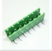
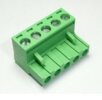
Looking at the two terminal block pictures, I assume the one with screws plugs into the one w/o screws?
I'm curious why you mention if the boards work.
This site uses cookies to help personalise content, tailor your experience and to keep you logged in if you register.
By continuing to use this site, you are consenting to our use of cookies.