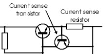
Variations of the two-transistor current-limit circuit (below) are often used where high-side current limiting is required. It can have either a BJT or MOSFET for the pass transistor, but they all use a BJT sense transistor, which turns on to limit the current when the voltage across the current-sense resistor reaches its ≈0.7V base-emitter voltage. This works fairly well as a simple current limit circuit but does have some significant limitations.

It causes up to a 0.7V drop in the protected circuit and has a -0.3%/°C negative temperature coefficient of the current limit value. It also cannot be readily adjusted over more than a small current range without changing the shunt resistor value, or set to zero current, as is often desired for adjustable/bench power supplies (such as one using an LM317 regulator).
Stable, low drop, current-limit circuits that can be adjusted over a wide range down to zero can be somewhat complex, often requiring a rail-rail op amp or some specialized IC.
The circuit discussed below meets those functional goals but avoids the complexity by connecting the emitters of a simple dual-PNP current-mirror across the current-sense resistor, where they function as a differential amp comparator. This provides detection of a small voltage across the high-side current sensing resistor and comparing it to a reference voltage to give a stable current limit.
It only requires a dual transistor, one MOSFET, one TL431 voltage reference, and a few passive components.
(A simplified alternate circuit without the TL431 reference but with reduced performance is shown at the end of this paper.)
Its voltage drop, when not limiting, is <100 mV, plus the IR drop through the MOSFET on-resistance.
Simulation--
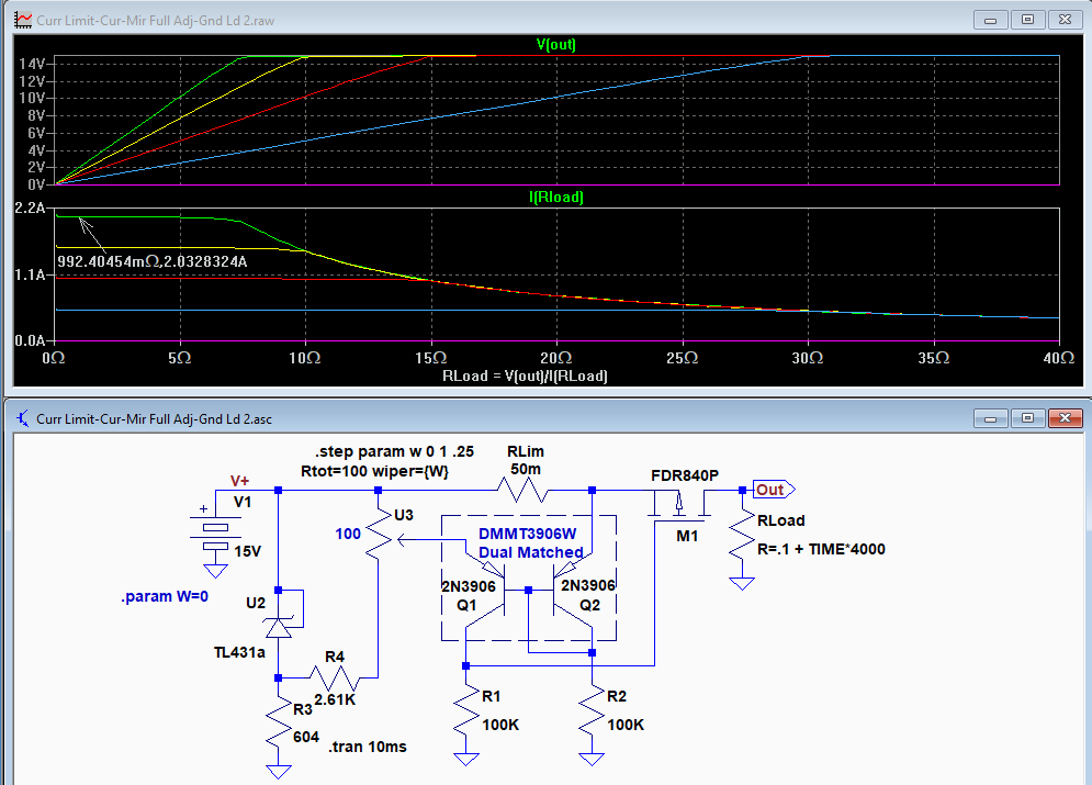
The LTspice simulation of the circuit is shown below for a load variation of 0.1Ω to 40.1Ω with the current-limit adjust pot going from 0% to 100% in 5 steps.
The current mirror circuit, Q1 & Q2, acts as a differential-voltage sense-amp across Rlim. When the voltage across Rlim due to the output current, reaches the U3 pot setting voltage, Q1 in the mirror starts to turn on. This raises the voltage across R1 which reduce Vgs of MOSFET M1, turning it off and limiting the output current.
The voltage for current-limit-adjust pot U3 is provided by the TL431 (U2) voltage reference. It generates a constant 2.5V between V+ and the junction of R3 and R4, to give a stable constant-current voltage setting.
This and the current-mirror differential configuration cancelling out nearly all the base-emitter voltage change means the current limit is quite stable with temperature change.
The RLim shunt resistor, 50 mΩ in the simulation, gives a current limit in I(RLoad), of zero to 2.0A maximum, by adjusting pot U3.

The P-MOSFET should be rated for the supply voltage used and have a low on-resistance at the maximum desired operating current.
If the supply voltage is below 10V, a logic-level type P-MOSFET should be used (with a Vgs maximum threshold of 2V or less).
Of course the dissipation in the MOSFET can be significant under limit, (Vin-Vout) x Iload), so it will need to be mounted on a heat-sink if it operates under limit conditions for more than a few seconds.
The value of the current sense resistor, Rlim can be changed if a higher current limit is desired.
U3 and R4 are configured for a maximum current sense voltage of ≈100mv, so the desired Rlim value = 100mV / Ilim(max).
This allows the use of standard 100 mV shunts.
For best operation the transistors in the current mirror, Q1 and Q2, should be matched.
The referenced DMMT3906W pair, which is basically two matched 2N3906's in one package, are inexpensive, selling for U$0.37 here, for example.
Typically this current limiter circuit would be connected between the input power and the regulator, so that it doesn't affect the output regulation.
Simplified Circuit--
Below is the LTspice simulation of a simplified version of the current-mirror limiter circuit.
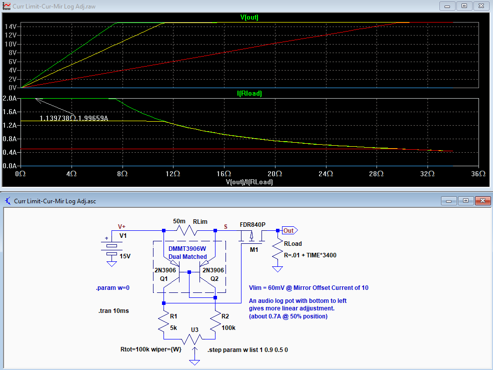
It biases the two transistors at a different current which generates a band-gap voltage difference between the Vbe voltages. This voltage is about 60mV for a 10:1 difference in current.
The main disadvantage of this circuit compared to the previous is, it has a temperature sensitivity of about -0.3%/°C for the current setting. If that's not an issue then this can be used in place of the previous circuit, thus eliminating the TL431 reference voltage.
The simulation below shows the current limit for pot settings of 0%, 50%, 90% and 100%, giving currents of 0A, 0.50A, 1.34A, and 2.00A.
This shows another disadvantage of this circuit compared to the previous, in that the current limit is basically a log function of the linear pot setting.
This can be made more linear by using a log (audio) pot rather than a linear pot, as noted on the schematic.
(Note that this connection will give the maximum voltage at the zero CW pot position. An antilog pot would reverse this, giving zero current at the zero position).
The maximum current limit is determined by the value of RLim and can be changed as needed.
Its value is ≈ 100mV / Ilim(max).

It causes up to a 0.7V drop in the protected circuit and has a -0.3%/°C negative temperature coefficient of the current limit value. It also cannot be readily adjusted over more than a small current range without changing the shunt resistor value, or set to zero current, as is often desired for adjustable/bench power supplies (such as one using an LM317 regulator).
Stable, low drop, current-limit circuits that can be adjusted over a wide range down to zero can be somewhat complex, often requiring a rail-rail op amp or some specialized IC.
The circuit discussed below meets those functional goals but avoids the complexity by connecting the emitters of a simple dual-PNP current-mirror across the current-sense resistor, where they function as a differential amp comparator. This provides detection of a small voltage across the high-side current sensing resistor and comparing it to a reference voltage to give a stable current limit.
It only requires a dual transistor, one MOSFET, one TL431 voltage reference, and a few passive components.
(A simplified alternate circuit without the TL431 reference but with reduced performance is shown at the end of this paper.)
Its voltage drop, when not limiting, is <100 mV, plus the IR drop through the MOSFET on-resistance.
Simulation--
The LTspice simulation of the circuit is shown below for a load variation of 0.1Ω to 40.1Ω with the current-limit adjust pot going from 0% to 100% in 5 steps.
The current mirror circuit, Q1 & Q2, acts as a differential-voltage sense-amp across Rlim. When the voltage across Rlim due to the output current, reaches the U3 pot setting voltage, Q1 in the mirror starts to turn on. This raises the voltage across R1 which reduce Vgs of MOSFET M1, turning it off and limiting the output current.
The voltage for current-limit-adjust pot U3 is provided by the TL431 (U2) voltage reference. It generates a constant 2.5V between V+ and the junction of R3 and R4, to give a stable constant-current voltage setting.
This and the current-mirror differential configuration cancelling out nearly all the base-emitter voltage change means the current limit is quite stable with temperature change.
The RLim shunt resistor, 50 mΩ in the simulation, gives a current limit in I(RLoad), of zero to 2.0A maximum, by adjusting pot U3.
The P-MOSFET should be rated for the supply voltage used and have a low on-resistance at the maximum desired operating current.
If the supply voltage is below 10V, a logic-level type P-MOSFET should be used (with a Vgs maximum threshold of 2V or less).
Of course the dissipation in the MOSFET can be significant under limit, (Vin-Vout) x Iload), so it will need to be mounted on a heat-sink if it operates under limit conditions for more than a few seconds.
The value of the current sense resistor, Rlim can be changed if a higher current limit is desired.
U3 and R4 are configured for a maximum current sense voltage of ≈100mv, so the desired Rlim value = 100mV / Ilim(max).
This allows the use of standard 100 mV shunts.
For best operation the transistors in the current mirror, Q1 and Q2, should be matched.
The referenced DMMT3906W pair, which is basically two matched 2N3906's in one package, are inexpensive, selling for U$0.37 here, for example.
Typically this current limiter circuit would be connected between the input power and the regulator, so that it doesn't affect the output regulation.
Simplified Circuit--
Below is the LTspice simulation of a simplified version of the current-mirror limiter circuit.
It biases the two transistors at a different current which generates a band-gap voltage difference between the Vbe voltages. This voltage is about 60mV for a 10:1 difference in current.
The main disadvantage of this circuit compared to the previous is, it has a temperature sensitivity of about -0.3%/°C for the current setting. If that's not an issue then this can be used in place of the previous circuit, thus eliminating the TL431 reference voltage.
The simulation below shows the current limit for pot settings of 0%, 50%, 90% and 100%, giving currents of 0A, 0.50A, 1.34A, and 2.00A.
This shows another disadvantage of this circuit compared to the previous, in that the current limit is basically a log function of the linear pot setting.
This can be made more linear by using a log (audio) pot rather than a linear pot, as noted on the schematic.
(Note that this connection will give the maximum voltage at the zero CW pot position. An antilog pot would reverse this, giving zero current at the zero position).
The maximum current limit is determined by the value of RLim and can be changed as needed.
Its value is ≈ 100mV / Ilim(max).


