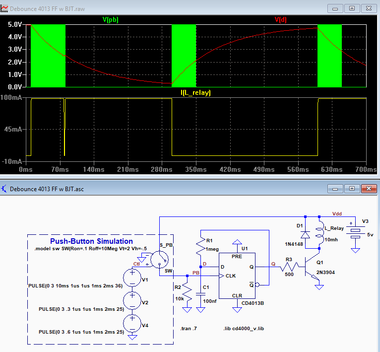
Here's a relatively simple circuit to give a latching relay function from a momentary, single-pole (SP) push-button operation.
It includes a simple RC circuit for debounce which ignores multiple pulses from a mechanical PB output, avoiding the more complex (RC diode, etc.) circuits often used for debounce of the signal from a mechanical switch.
The circuit below consists of a CD4013 CMOS D-FF connected as a toggle latch, controlling a BJT that drives the relay coil.
Debounce is provided by R1C1.
After the first contact bounce clocks the FF to its opposite state, it ignores subsequent bounce pulses until the D input has reached the opposite logic state voltage level (≈50% of Vdd) with delay ≈0.7 R1C1.
The LTspice simulation shows the relay coil current for two different durations of input bounce signals.
The first period shows the FF changing state at the start of the sequence and again after ≈68ms of bounce signals.
That should be adequate since most switch bounce durations are typically less than this but, if not, the R1C1 value can be increased as needed.
The second and third 50ms periods of bounce signals give a clean, single change of state at the start of each period, as expected.
Power and ground for the CD4013 are not shown, and all unused inputs for the other FF in the package must be grounded.
The circuit can operate at up to 15V supply (with an appropriate increase in the value of R3).

