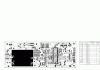
So I found out that I botched a PCB but it's too late to cancel the order now so I gotta live with it. Well...when I found out I had botched it and had to make corrections and I ended up also adding a bunch of other stuff which means I will send away for a good board again anyways (another $100, ack). So now I have to salvage this PCB.
Anyways, it's a dsPIC control board for a chip with SPI/i2C/Programming/Emulation lines multiplexed to the same pin (with the emulation lines also multiplexed to a separate set of pins). What the board does it has a DPDT switch that is *supposed* to let you program the device, but then transfers the ICD jack to the emulation pins so you can debug with
I2C devices connected to the sytem.
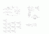
My switch arrangement:
Switch Position 1- ICD2 jack -> I2C/Programming pins
Switch Position 2- ICD2Jack -> Emulation Pins
What I did not realize is that there is no harm sending programming messages to the emulation pins while programming. I also forgot about the pull-up resistors on the I2C lines which is not so bad since I can plug them externally into the I2C jack. The big problem is that for programming to work properly, I must basically unplug all I2C devices and the pull-up resistors from the I2C jack since these will prevent the ICD2 from programming properly.
Correct Switch Arrangement:
ICD2 Jack- Hardwired to Emulation Pins
Switch Position 1- programming/I2C pins -> ICD2 Jack
Switch Position 2- programming/I2C pins -> I2C port (and pull-up resistors)
So basically, what it boils down to is that for I2C to work I have to add to plug external pull-up resistors into the I2C jack which isn't too bad. But the switch does not disconnect the pull-up resistors (or I2C devices) from the programming/I2C pin when I need to program. It's just a pain.
Can anyone think of any way around this short of unplugging everything from the I2C jack every time I need to program? I'm pretty sure there's no way around it, so something like the suggestion of a jack that can be disconnected by a electrically disconnected by a button (but physically still connected) would be nice.
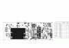
Anyways, it's a dsPIC control board for a chip with SPI/i2C/Programming/Emulation lines multiplexed to the same pin (with the emulation lines also multiplexed to a separate set of pins). What the board does it has a DPDT switch that is *supposed* to let you program the device, but then transfers the ICD jack to the emulation pins so you can debug with
I2C devices connected to the sytem.
My switch arrangement:
Switch Position 1- ICD2 jack -> I2C/Programming pins
Switch Position 2- ICD2Jack -> Emulation Pins
What I did not realize is that there is no harm sending programming messages to the emulation pins while programming. I also forgot about the pull-up resistors on the I2C lines which is not so bad since I can plug them externally into the I2C jack. The big problem is that for programming to work properly, I must basically unplug all I2C devices and the pull-up resistors from the I2C jack since these will prevent the ICD2 from programming properly.
Correct Switch Arrangement:
ICD2 Jack- Hardwired to Emulation Pins
Switch Position 1- programming/I2C pins -> ICD2 Jack
Switch Position 2- programming/I2C pins -> I2C port (and pull-up resistors)
So basically, what it boils down to is that for I2C to work I have to add to plug external pull-up resistors into the I2C jack which isn't too bad. But the switch does not disconnect the pull-up resistors (or I2C devices) from the programming/I2C pin when I need to program. It's just a pain.
Can anyone think of any way around this short of unplugging everything from the I2C jack every time I need to program? I'm pretty sure there's no way around it, so something like the suggestion of a jack that can be disconnected by a electrically disconnected by a button (but physically still connected) would be nice.
Last edited: