Continue to Site

Welcome to our site!

Electro Tech is an online community (with over 170,000 members) who enjoy talking about and building electronic circuits, projects and gadgets. To participate you need to register. Registration is free. Click here to register now.

  • Welcome to our site! Electro Tech is an online community (with over 170,000 members) who enjoy talking about and building electronic circuits, projects and gadgets. To participate you need to register. Registration is free. Click here to register now.

Connecting nets in Eagle, finding a symbol

Status
Not open for further replies.

edeca

Active Member
In the following example, the DAT/CLK/OE/LAT pins of the two shift registers are connected to the PIC RB* pins:

**broken link removed**

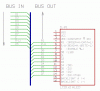
I did this by naming the nets the same and I have verified it by checking that it is turned into a trace on the board.

However, this isn't very clear. Is there some sort of symbol I can put on the schematic to show that these pins are connected, like the +5V and GND ones that I have used elsewhere? I can't seem to find one.

This would make the schematic much cleaner (and yes, I need to fix that bus at the top, it's ugly!).

Eagle parts for the three items in the PCB are available **broken link removed**, I'd love critique or comments.
 
Last edited:
Hi edeca,

Do the following steps for a neat schematic:

Grid size 0.025", size (letters) 0.056", ratio (standard 8) 6, layer95 (names). Click the symbol marked "ABC" (Label).

Next click the net you want to label and place the label at the selected position.

The bus "SOURCE[0..7]" is not only ugly, but unnecessary.

Buses make sense if many ICs on the board use the same signals, e.g. CLK, \CS, DATA[0..7] etc. Connect nets directly and label them properly instead.

When using buses you might label them as well to make reading of the schematic easy.

Boncuk
 

Attachments

  • LABEL-01..gif
    LABEL-01..gif
    6 KB · Views: 238
  • BUS..gif
    BUS..gif
    10.8 KB · Views: 305
Last edited:
Do the following steps for a neat schematic:

Grid size 0.025", size (letters) 0.056", ratio (standard 8) 6, layer95 (names). Click the symbol marked "ABC" (Label).

Thanks bonc, that's brilliant. See the image below for how I am getting on.

Schematic-Rev1..png

I just need to get rid of that bus at the top right now, but the pins are the wrong way round. Any ideas?

Critique of other elements gladly received. I'm not sure I like the way I have done the ICD connector. But I like having the PIC, PSU and output separate. That means I can reuse pieces more easily and I can provide images of small parts of the circuit on their own for when I document it.
 
Hi edeca,

please zip your schematic and post it. I'll check for possibilities to connect the MIC5891 and the lines of the matrix properly without using a bus.

Boncuk

BTW, I don't like the bulky flags. :rolleyes:
 
Last edited:
Status
Not open for further replies.

Latest threads

New Articles From Microcontroller Tips

Back
Top