Continue to Site

Welcome to our site!

Electro Tech is an online community (with over 170,000 members) who enjoy talking about and building electronic circuits, projects and gadgets. To participate you need to register. Registration is free. Click here to register now.

  • Welcome to our site! Electro Tech is an online community (with over 170,000 members) who enjoy talking about and building electronic circuits, projects and gadgets. To participate you need to register. Registration is free. Click here to register now.

Design a sydouble power supply

Status
Not open for further replies.

Melfior_Ra

New Member
Hi all.

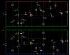
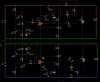
I am a self learner, I started study electronics 2 years ago an now I want to put into practice what i have learnt. I want to design (and build) a double power using op amps, and transistors.
I want to be short circuit and overload protected between 1.5 -2.5 amps. I simulated the design in Circuit Wizard which helps me a lot to understand current flow and voltages (honestly it is a noob friendly :D ). The circuit seems to work ok but i do not have experience in choosing components (i know how to look into a datasheet but i do not have all the knowledge to understand everything). So please look at my design and if you find something faulty or you think it needs improvements let me know.
Thank you in advance.

PS.
VR3 AND VR7 simulates the loads
 

Attachments

  • dual power supply.jpg
    dual power supply.jpg
    135.1 KB · Views: 156
when sizing components you have to look at datasheets of used components. for example MJE3055 is power transistor which means it can handle high power but power transistors are notoriously bad when it comes to amplification. this one (which is common for power transistors) has gain of only 20 (granted, this is in worst case), lookup hfe or "DC Current Gain"
https://www.electro-tech-online.com/custompdfs/2013/02/MJE3055.pdf

this means that to get 2A through this transistor, you need at least 2A/20=0.1A current through it's base. you should be able to test this when VR3 is set to more reasonable value such as 5 Ohm. 0.1A into base means 0.1A out of opamp. that is 100mA or about 5x more than LM358 will handle. i would strongly suggest adding another (smaller) transistor as buffer.

next problem is that you use same IC (which has two opamps but they are powered from same terminals), and you connect it to different power rails. this can work if you use two separate chips or you need to rearrange power for opamps.

next is the location of current sensing (it is not good choice). issue is that if load current changes (which is common) voltage drop on 0.47 Ohms will change and your output voltage will change by up to 0.7V. that is way too much for regulated power supply. maybe one tenth of that would be tolerable. there are different ways to solve it. probably simplest is to just change where you measure output voltage so that voltage drop due current sensing is automatically compensated for. just move top side of R4 (and bottom side of R11) directly to the output terminal (after 0.47 Ohm).
 
thank you a lot.

I made the modifications in the design. I understood everything what you said but can you please explain in detail why is better to include the sense resistor in feedback path?

Can i build now ? ;)

Thanks
 
Maybe a few questions before you start.

What minimum and maximum voltage do you want and what current at each voltage?
I ask this because the power in the 3055 may be very high at low voltage and high current.

As pointed out above by panic mode the LM358 can not supply enough current to make the 3055 turn on for 2 amps. In the data-sheet for the 3055 this is called DC current gain. In the 358 data sheet It is called output source and sink current. So if the 358 can put out 10 ma and the gain of the 3055 is only 20 you will only be able to draw 0.2 amps. In reality it will do better than that but maybe not much. You can probably add a transistor after the 358 to get more power.
 
...why is better to include the sense resistor in feedback path?

Most of modern circuits use some degree of digital logic (TTL, CMOS, microcontrollers, etc.). Quite few of them are rather picky about operating voltage. For example TTL expects 4.75-5.25V and most of the chips list some max limit like 6V etc. The point is that small change such as moving from 5V to 5.25V means you are out of spec. and moving from 5.25V to 6V could mean that your hardware suffered damage or is destroyed. Many things are using different voltages but it is usually 5V and less that is very sensitive to voltage changes or transients. you can also compare what is standard in the inductry, you don't want your fancy PSU to be an laughing stock of everyone who made a regulated power supply in their life. For example LM7805 states output tolerance of +/-2% which translates to +/-0.1V (or +/-4% over rated temperature range). This is a very old regulator, many others are better (LM317 is 0.3% etc.). If 7805 could not get the output to be within commonly required 4.75-5.25V, it would be worthless piece of cr@p and nobody would want it. The whole point of voltage regulation is to make a power supply where voltage is (and remains) constant - NO MATTER WHAT! This also means regardless if you draw 1mA, 500mA or 2.5A. Ok with this? Good...

Key points:
1. getting PERFECTLY stable output is impossible (but we try and get close)
2. even when we REGULATE voltage, we STILL have SOME deviation of the output voltage.
3. things that are called regulators but don't regulate very well are bad (if it is possible to regulate better, then replace "bad" with "junk").
4. to get regulation, we need reference and feedback
5. any resistance after regulator creates ADDITIONAL fluctuations in output voltage (because now the output is not output of the regulator but point after that resistance).


Voltage divider chains such as R4-VR1-R5 are key part of the feedback loop. They are used to measure voltage at some point. If voltage at THAT point is below reference, regulator increases output to compensate. If voltage at THAT point is above reference, regulator decreases output to compensate. This process is called closed loop and corrects voltage (which is what regulation should do) at THAT point. The only problem is that that is the WRONG point. We don't care that our circuit makes voltage stable at SOME point. We want that to be at the PSU output.
 
Can i build now ? ;)

Are you asking me for permission? :rolleyes:

Seriously, I don't see any obvious problems but it's 2AM here and I also don't know what your comfort level is or what kind of mistakes you may end up making. But...even if it blows up and you have to start again, I can't see you locating me and knocking up on my door so... Should I care? :p
 
Thank you very much.

I am not asking you the permision, but i made the changes in design and i posted the image of the new circuit but it is not here and i dont know why. And please excuse my english.
Ohhh.. about knocking .... who knows it is a small world :D :D :D
 
if you have trouble posting here, yo may try sites like www.use.com (it is free and simple and does not require registration). then you just post link.
 
Status
Not open for further replies.

Latest threads

Back
Top