Continue to Site

Welcome to our site!

Electro Tech is an online community (with over 170,000 members) who enjoy talking about and building electronic circuits, projects and gadgets. To participate you need to register. Registration is free. Click here to register now.

  • Welcome to our site! Electro Tech is an online community (with over 170,000 members) who enjoy talking about and building electronic circuits, projects and gadgets. To participate you need to register. Registration is free. Click here to register now.

Emitter follower with split supplies

Status
Not open for further replies.

bakkis

New Member
Hi,
I was reading Art of electronics, chapter 2: Some basic transistor circuits. In section 2.05 - Followers with split supplies, i find this paragraph little confusing:

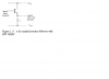
Because signals often are "near ground," it
is convenient to use symmetrical positive
and negative supplies. This simplifies
biasing and eliminates coupling capacitors
(Fig. 2.17).

I have attached the Figure. Could somebody explain How using split supply simplifies biasing and eliminates coupling capacitors ?
 

Attachments

  • EmitterFollower.png
    EmitterFollower.png
    18.3 KB · Views: 286
hi b,
Consider the case where that circuit had a single positive supply.

In order to reproduce a close to ground low level input sine wave signal to the base, at the emitter, the designer would have to consider the effect of the required Vbe voltage.

For the transistor to be biased ON, Vbe would have to be approx +0.65V, so this would mean the input signal would have to be superimposed upon this Vbe voltage.
To do this the designer would have to AC couple the low level signal and apply a bias current into the base of the transistor, to bring it into is operating/linear conduction.

By adding this bias and Vbe the transistor will be conducting and there will be a voltage drop across the emitter resistor.
Assuming the bias is correctly set this would mean the output sine wave is superimposed upon the emitter voltage.

By using dual supplies the bias and operating point of the transistor can be chosen to avoid the need for AC coupling and the biasing.

Do you follow that OK.?

EDIT:
Added images.
 

Attachments

  • AAesp01.gif
    AAesp01.gif
    47.2 KB · Views: 374
Last edited:
Hi eric,
Thank you so much. Yes, i followed the biasing part very well. I had missed the Vbe. However, i still do not understand the AC coupling part. Now, coupling capacitor is used for blocking DC component,how does this fit in ?
 
Last edited:
Status
Not open for further replies.

Latest threads

New Articles From Microcontroller Tips

Back
Top