I've been designing a simple dual FET Wheatstone bridge using the website "www.falstad.com/" which allows one to draw a circuit very easily and it shows how it runs and does all the calculations. It's very simple to use.
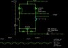
I've attached a pic of a typical circuit.
The transistors used in the simulation are supposed to be MPF102 n-JFETs, with Vp= -8V, and a 20mA limit.
By playing with bias resistor values, I've gotten some unusual results.
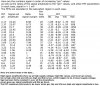
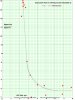
The attached graph and table of my data shows a range of values for FET gain, gm, and the signal amplitudes I got for each circuit I tried.
In the very high signal amplitude circuits, the resistor settings are extremely touchy. Small changes can send the amplitude from the mV range down to the uV range.
I thought gain above 5, or so, was not possible with FETs, so my questions are:
1. These high signal amplitudes don't seem possible, are they a fluke of the calculations?
2. Why should circuits with low FET gain, gm, have high signal amplitudes and vice-versa?
3. Why don't the circuits with the highest gm have the highest signal amplitudes?
4. Looking at the chart, which values should I strive for? High gm but lower signal amplitude (assuming these amplitudes are actually possible)? Or, low amplitude, with high gm value?
Or, should I look at some combination of the other FET parameters?
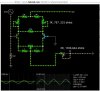
I've attached a pic of a typical circuit.
The transistors used in the simulation are supposed to be MPF102 n-JFETs, with Vp= -8V, and a 20mA limit.
By playing with bias resistor values, I've gotten some unusual results.
The attached graph and table of my data shows a range of values for FET gain, gm, and the signal amplitudes I got for each circuit I tried.
In the very high signal amplitude circuits, the resistor settings are extremely touchy. Small changes can send the amplitude from the mV range down to the uV range.
I thought gain above 5, or so, was not possible with FETs, so my questions are:
1. These high signal amplitudes don't seem possible, are they a fluke of the calculations?
2. Why should circuits with low FET gain, gm, have high signal amplitudes and vice-versa?
3. Why don't the circuits with the highest gm have the highest signal amplitudes?
4. Looking at the chart, which values should I strive for? High gm but lower signal amplitude (assuming these amplitudes are actually possible)? Or, low amplitude, with high gm value?
Or, should I look at some combination of the other FET parameters?