Continue to Site

Welcome to our site!

Electro Tech is an online community (with over 170,000 members) who enjoy talking about and building electronic circuits, projects and gadgets. To participate you need to register. Registration is free. Click here to register now.

  • Welcome to our site! Electro Tech is an online community (with over 170,000 members) who enjoy talking about and building electronic circuits, projects and gadgets. To participate you need to register. Registration is free. Click here to register now.

Interpretation of LTspice circuit

Status
Not open for further replies.

sallehzxc

New Member
Hi guys!

I have recently changed my schematic to reflect the non-ideal nature of the passive filters in the circuit (aka inductor and capacitor).

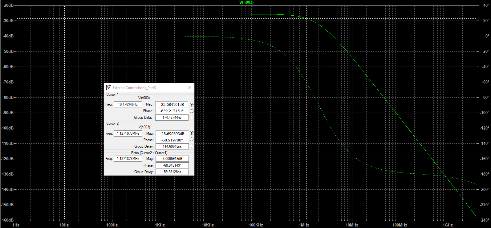
the output graph, taken at the node at the end seems to mimic a low pass filter but my desired output is with regards to an output of 30MHz and the concern i have is with regards to the harmonics of my carrier frequencies, thought of to be 24MHz, 102 and 360 MHz affecting and distoring my signal.

Sadly i have no idea how to interpret the graph.

Can anybody aid me and share their insight on my circuit?

1537951984782.png


1537952058870.png


am i also right to say that the cut-off freq, at 3db, is 1.2719MHz.

Thank you in advance.

This forum has been amazing!
 
I changed the "ESR" on V1. Most signal generators have a impedance of 50 ohms. Look at the graph. First point is 50 ohms and 1nF. Next point is L2 and C4. Then L3 and C3. The coils ring pretty bad.
1538014269399.png

Next: I change C1 to 1pf to show what that does. Now the 50 ohms and 1pF does nothing. You can see the two points where the curve changes slope.
1538014524448.png

What are you doing with the filter?
 

Attachments

  • 1538014238964.png
    1538014238964.png
    8.5 KB · Views: 279
HI Ron! Thanks for the reply and aid.

The initial signal ( symbolised as the signal gen) is meant to come from an acquisition board so thus i am unsure of the internal resistance present.
Thus for my scenario, i am assuming that it just comes in as signal sweep.

The filter for my design was meant to filter out a signal such that it can be used as a ref signal for my ADF4350 chip to be used.

I took a look at the schematic again and realised that there were some additional values attached (i will attach the file here if you have any comments for me).
Again, I am not sure what to make of it when i look at the graph output (note, this was a design by passed on to me to justify) so i am assuming the filter is meant to filter out any harmonics of carrier signal present so that the signal inputted is not distorted.

1538016397892.png


There also seems to be a lot of noise coming from just outside the sig generator in this case. thank you again for your advise and maybe i am missing something in my simulations of justifying my mentors supposedly working circuit.
 

Attachments

  • ExternalConnections_Part1.asc
    1.7 KB · Views: 280
Status
Not open for further replies.

Latest threads

New Articles From Microcontroller Tips

Back
Top