KansaiRobot
Member
Hello and thanks always.
So ar I have worked only with schematics and on the implementation part with breadboards and perfboards. I would like to learn the theory behind designing PCBs. I am not right now thinking of actually "making" them but learn how to design the layouts, the artwork etc. (since my knowledge is nil I dont know if I am using the correct terminology).
Can anybody advice me on links, tutorials, books or any resource for this?
For example I would like to understand the following terms:
FR-1, FR-3 CEM-3 FR-4
Surface treatement : lead-free soldering leveler, Soldering leveler , stripping beaten copper, Flux processing, Golden flash
Number of layers, Signal layer, Power supply layer
PhotoSR PrintingSR Parts surface, Solder surface
Silk
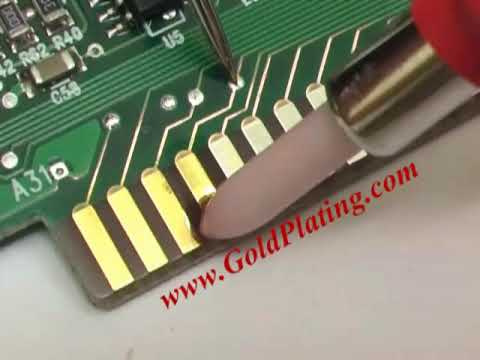
Gold platting
Board processing, v-slit processing, Perforation processing, Router processing
Artwork drawing
Garber data
RoHS, UL, CE
etc.
Thanks in advance
So ar I have worked only with schematics and on the implementation part with breadboards and perfboards. I would like to learn the theory behind designing PCBs. I am not right now thinking of actually "making" them but learn how to design the layouts, the artwork etc. (since my knowledge is nil I dont know if I am using the correct terminology).
Can anybody advice me on links, tutorials, books or any resource for this?
For example I would like to understand the following terms:
FR-1, FR-3 CEM-3 FR-4
Surface treatement : lead-free soldering leveler, Soldering leveler , stripping beaten copper, Flux processing, Golden flash
Number of layers, Signal layer, Power supply layer
PhotoSR PrintingSR Parts surface, Solder surface
Silk
Gold platting
Board processing, v-slit processing, Perforation processing, Router processing
Artwork drawing
Garber data
RoHS, UL, CE
etc.
Thanks in advance