Hi,
I'm designing a PCB for a GPS receiver. On the gps datasheet, they request that the trace that will connect the antenna pin (active antenna) and the antenna connector (as well as antenna cable and antenna connector) have a 56ohms impedance.
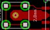
I've used the AppCad program from Agilent to calculate the trace width of that trace. I've input all the parameters (pcb material, board height, copper thickness, signal frequency, etc) and it gave me a reccomended trace width of 2.8mm.
The problem I'm having is that the antenna connector (smb) has the signal pin in the center and 4 supporting ground pins on each side of the connector. I'm not neither I can use more than 2 layers, and I'm afraid that if I use vias to transpose the microstrip to the bottom layer, the via won't have the correct impedance.
Therefore I have two alternatives: 1) to "choke" the signal in between two ground pins, and 2) to decrease the trace width to 2mm
I don't know which one is the worst... if I decrease the width to 2mm, the calculated impedance will be 60ohms. If I leave it at 2.8mm but and make it thinner to pass the ground pins, I'm not sure if impedance will be kept at 50ohms or even worse, if the irregular shape of the trace won't be even worse for the signal (is there such a thing as signal reflecting on the edges of the trace?)
Appreciate your comment.
I'm designing a PCB for a GPS receiver. On the gps datasheet, they request that the trace that will connect the antenna pin (active antenna) and the antenna connector (as well as antenna cable and antenna connector) have a 56ohms impedance.
I've used the AppCad program from Agilent to calculate the trace width of that trace. I've input all the parameters (pcb material, board height, copper thickness, signal frequency, etc) and it gave me a reccomended trace width of 2.8mm.
The problem I'm having is that the antenna connector (smb) has the signal pin in the center and 4 supporting ground pins on each side of the connector. I'm not neither I can use more than 2 layers, and I'm afraid that if I use vias to transpose the microstrip to the bottom layer, the via won't have the correct impedance.
Therefore I have two alternatives: 1) to "choke" the signal in between two ground pins, and 2) to decrease the trace width to 2mm
I don't know which one is the worst... if I decrease the width to 2mm, the calculated impedance will be 60ohms. If I leave it at 2.8mm but and make it thinner to pass the ground pins, I'm not sure if impedance will be kept at 50ohms or even worse, if the irregular shape of the trace won't be even worse for the signal (is there such a thing as signal reflecting on the edges of the trace?)
Appreciate your comment.