Continue to Site

Welcome to our site!

Electro Tech is an online community (with over 170,000 members) who enjoy talking about and building electronic circuits, projects and gadgets. To participate you need to register. Registration is free. Click here to register now.

  • Welcome to our site! Electro Tech is an online community (with over 170,000 members) who enjoy talking about and building electronic circuits, projects and gadgets. To participate you need to register. Registration is free. Click here to register now.

My first Eagle schematic and board

Status
Not open for further replies.

antknee

New Member
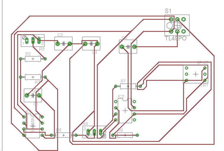
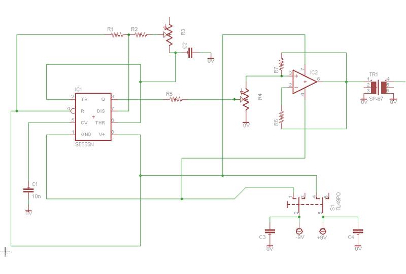
I have made up my first Eagle schematic and board and would welcome some feedback.

The circuit is a 555 timer going into an opamp and then a transformer. It works on a stripboard so I'd like to get it made up professionally and have a company in mind. I have made a few changes from the stripboard, in particular I've made the circuit dual supply. I've also added some supply bypass capacitors. The opamp is a servo with a slightly unusual feedback config. Eagle says the board and schematic have no errors and are consistent.

I'm struggling with how to add power planes so I've left the board big while I work out what i'm supposed to do. I get some warnings saying "Power pin IC1 Gnd connected to net N$3" and "Power pin IC2 V+ connected to N$5". I'm not sure what exactly they mean.

Thanks.
untitled-2-jpg.43774


untitled-1-jpg.43773
 

Attachments

  • Untitled 1.jpg
    Untitled 1.jpg
    51.4 KB · Views: 1,634
  • Untitled 2.jpg
    Untitled 2.jpg
    27.7 KB · Views: 1,888
The warning is not problem, it's just telling you that the ground pin of the 555 is not connected to a net named ground. But you do have it connected to the lowest potential in the circuit through a switch. One thought though. You are running the 555 at its absolute maximum rating of 18V. Not sure if that is good. Does it get hot at all?
 
R6 looks funny like it is shorted? Maybe it is just me?

Ron
 
Glad to see you are giving it a go.

You are using through hole parts and routed the traces on the top (red) layer. Use the bottom (blue) layer instead.

Do not use the auto router. You can do so much better yourself.
 
I would also check your trace widths. Use this calculator:
PCB Track Width Calculator
They look like they are one of the smallest widths, which means they can't handle alot of current. I don't know exactly what you are making, but they look small to me.

Mike
 
Note two points:The trace of single layer PCB should be drawn on bottom layer [solder layer];
The trace width as wide as possible.
 
You are running the 555 at its absolute maximum rating of 18V. Not sure if that is good. Does it get hot at all?

Would putting some resistors in series with the power input pins save power? I could lower the input power and up it again at the opamp.
 
R6 looks funny like it is shorted? Maybe it is just me?

Ron

It does look funny, I hadn't noticed. I will check.

You are using through hole parts and routed the traces on the top (red) layer. Use the bottom (blue) layer instead.

Do not use the auto router. You can do so much better yourself.

Will do. I read a tutorial which said use one layer if possible, I didn't put any thought into which.

I would also check your trace widths. Use this calculator:
PCB Track Width Calculator
They look like they are one of the smallest widths, which means they can't handle alot of current. I don't know exactly what you are making, but they look small to me.

Mike

Thanks for the link. That is a good idea, I would also like to make the pads/pins bigger.
 
Last edited:
The 45-degree trace better than 90 degree's. There are too sparse place, you should move to a little tight, reducing the PCB area.
 
The trace is hidden under the resistor, so it is ok, thanks.

I'm still trying to find out how to add the power planes. I click on polygon and create an area bounded by dotted lines and I cant figure out which commands to give next. Or where to put the polygon....
 
You should check the +-9v Net name in the SCH & PCB , Do they have the same name?
 
Yes they have the same name. I think the problem is more the sequence of commands I give. I only need a plane for ground so i think it is

Draw a big polygon around the whole circuit
Type poly gnd .... ?
Click somewhere... ?

:)
 
Last edited:
You got the first part right presuming you have moved your traces to the bottom layer (blue) make your polygon around the whole circuit making sure it is also using the bottom layer and change its name with the same net name as your -9V and then click on "Ratsnest" and you should get a good view of it. Just try to have it so that all of it is connected, in other words there should be no islands.

Mike
 
Last edited:
The ratsnest button was what I was looking for, it worked a treat.

I have been playing around with Eagle and come to some conclusions. The first being that the only reason I got autoroute to work at 100% was because the traces were tiny at 0.2mm. The second being it just isn't possible to make this circuit with one side without it taking longer than I have.

I think I have to look at "vias" that will take current from one side of the board to the other. Is that right?

What sort of trace width would be sensible for 1A. The trace width calculator mentioned by mgeno returns two results, one at 0.4mm for internal traces and 0.15mm for external ones. What is the difference between internal and external?

Thanks.
 
Last edited:
Would putting some resistors in series with the power input pins save power? I could lower the input power and up it again at the opamp.

I don't know if putting resistors in series would help you. It's not so much a question of power savings. It's just that you are running the 555 at it's absolute maximum voltage rating and generally, that's something I try to aviod. Maybe I'm being too conservative and someone else can chime in and tell you it's fine. Personally, I would decrease the supply volatge of the 555 and up the gain on the op amp to achieve your desired output. But if you have tested the circuit and everything works well without getting hot, it's probably OK.

What sort of trace width would be sensible for 1A. The trace width calculator mentioned by mgeno returns two results, one at 0.4mm for internal traces and 0.15mm for external ones. What is the difference between internal and external?

You will have external traces. Internal traces are traces sandwiched between the layers of a multi-layered board. Basically, they are inside the PCB. The trace widths are larger for internal traces over external traces because internal traces are not exposed to the air and therefore have a lesser ability to dissipate heat.
 
Last edited:
I don't know if putting resistors in series would help you. It's not so much a question of power savings. It's just that you are running the 555 at it's absolute maximum voltage rating and generally, that's something I try to aviod. Maybe I'm being too conservative and someone else can chime in and tell you it's fine. Personally, I would decrease the supply volatge of the 555 and up the gain on the op amp to achieve your desired output. But if you have tested the circuit and everything works well without getting hot, it's probably OK.

The switch is a momentary so the circuit hasn't been tested for long, I think the 555 would get hot but I wouldn't have noticed, I thought of resistors in series to reduce the voltage whereas now I think pots would be better.
You will have external traces. Internal traces are traces sandwiched between the layers of a multi-layered board. Basically, they are inside the PCB. The trace widths are larger for internal traces over external traces because internal traces are not exposed to the air and therefore have a lesser ability to dissipate heat.

So it is perfectly ok to use traces of 0.2mm at 1A. What seems small isn't that small.
 
I have finished.

I think I will end up shorting out the resistors I added to reduce volts for the 555 and living with the heating. That isn't the best outcome, I just think it is better to get this ordered, because there are probably quite a few things wrong with it, there are no mounting holes for example. When I have it the problems will be easier to see. I'm encouraged because it is a lot smaller than what I've been working with, about 5cm x 6cm. I can shrink it more later too.

Thanks for the input.

final-jpg.43813
 

Attachments

  • final.jpg
    final.jpg
    28.2 KB · Views: 1,046
Just a few points, not intended as criticism but things you could improve:

  • Get rid of all 90 degree corners, they are really bad on PCBs.
  • Watch how close your tracks are to pads, it is really easy to think there is a huge gap when zoomed in 100x. Look for example at C3.
  • Try and make it look pretty! Making PCBs is an artform. "Good enough is perfect" as one forum member says, but that's no reason not to think about lining up components or making the board as compact as possible.

Some of your ICs do not have all leads connected, is this intentional?
 
I was wondering about the 90 degree corners, I can miter them.

I have wires at 0.3mm and clearance at 0.9mm with no errors. I'd prefer wider traces but it causes too many warnings upping that and i've done a fair amount of reworking already.

I am the type of person who will spend forever looking for perfection, I enjoy it. I have to caution myself not to take that too far or I end up never getting anything done. I have already decided after this one arrives I will be making another, that is better and prettier :)

IC4 is a transformer with output lead not connected. The schematic I posted hasn't changed much it was a transformer there, it can be hard to find the right pad layout. IC2 is a dual opamp and I'm using just one of the amps.

Thanks for your input it was helpful.
 
Last edited:
Status
Not open for further replies.

New Articles From Microcontroller Tips

Back
Top