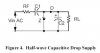
The circuit shown is a half wave capacitive drop circuit that is essentially a voltage divider such that a series capacitor drops an inputs voltage to more usable level.
Some circuit description,
Positive Half Cycle
-Ac Current flows through Rf,C1,D and parallel of C2 and RL.
-C2 been charged to one diode below the zener voltage, the current will have another parallel path in which to flow, C2 remains charged.
-C1 being charged during this time to a high voltage state
Negative Half Cycle
C1 discharged from the forward bias of zener diode
As an engineering rule of thumb, this approach can provide a load current of 10mAdc for each 1micro farad of ac capacitance.
Above are the information provided on the web, here is my question,
For positive half cycle,
1. How a zener diode is being turned-on? it mentioned there that is due to the C2 but i cant really understand it.
2. What is the another parallel path it mentioned? the loop that passed through the D,C2,and zener diode?
3. C1 is being charged to a high voltage state, the high voltage here meant te voltage that is nearly equal to input voltage?
For the circuit, isnt it the charging of C2 is only purposely for turning the zener diode on? How it discharge?
may i know what it meant by "according to the enginnering rule of thumb", it is a formula for calculating the value? what is the formula?
OK that's the problem i facing now, Pls help me... i am a newbie in this electronic things. Thankz...
Attachments
Last edited:

