Continue to Site

Welcome to our site!

Electro Tech is an online community (with over 170,000 members) who enjoy talking about and building electronic circuits, projects and gadgets. To participate you need to register. Registration is free. Click here to register now.

  • Welcome to our site! Electro Tech is an online community (with over 170,000 members) who enjoy talking about and building electronic circuits, projects and gadgets. To participate you need to register. Registration is free. Click here to register now.

Power Supply Instablity

Status
Not open for further replies.

Overclocked

Member
I just finished building a PSU using the LM2679. It works, But only if Unloaded. As Soon as I load it down, I get 10 to 12mV Of output. Is there anything I can do to fix this? The Output also takes time to recover if I short it out.

My Input ranges from 11.46V to 16.46V. Output is from 1.2V to 13.6V, and I tested a load across all ranges (first 4 ohms, then 6 ohms).

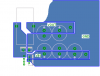
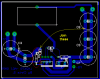
Im including the schematic and PCB (along with proper libraries) in eagle PCB format. Maybe theres an Error or something Im not seeing.

ADD: i have no clue what all those files are in the project folder, So I'll include those too.
 

Attachments

  • Vairable SMPS.zip
    535.4 KB · Views: 230
The fact that you've got R2 going to ground instead of the output doesn't make sense. You have no feedback loop. Comparing yours to the application note shows the difference:
 

Attachments

  • LM2679.PNG
    LM2679.PNG
    17.4 KB · Views: 660
  • Yours.png
    Yours.png
    7.5 KB · Views: 468
Last edited:
kchriste said:
The fact that you've got R2 going to ground instead of the output doesn't make sense. You have no feedback loop. The application note shows this:

Theres a Pot Connected from feedback to V+ Thats not shown on the schematic. Its in the PCB. I used 2 wires to connect it rather than on the board, which is why its not shown. Eagle is strange in the way that if you add inputs or output on the board, they dont reflect back into the schematic.

Also, C1 is Cboost, R2 is feedback, R1 is Radj, and C5 is Soft Start
 
By V+ I assume you mean the junction of C7-9 and the inductor?
EDIT: I've also noticed that there is no trace between the minus leads of the input caps ( C3&4) and the output caps (C7,8&9).
You should look at better component placement. If you move things around a bit, the trace from R2 doesn't have to meander all over the place:
 

Attachments

  • NewR2.png
    NewR2.png
    18 KB · Views: 247
Last edited:
kchriste said:
By V+ I assume you mean the junction of C7-9 and the inductor?
EDIT: I've also noticed that there is no trace between the minus leads of the input caps ( C3&4) and the output caps (C7,8&9).
You should look at better component placement. If you move things around a bit, the trace from R2 doesn't have to meander all over the place:

Hi kchriste,

I agree that it would be better to relocate R2; there's no reason I can see for it to be where it is. A bit south of the switcher might be easier. Also, removing the little traces and rearranging a bit lets you move the diode a bit away from the switcher, which might help with heat issues. I haven't calculated that, but it seems like it might be an issue.

If you load the board and run ratsnest, it joins the caps with a ground pour. I think the "little traces" might be there to try to link the grounds, but they are actually not required.

Overclocked, don't get me wrong--I'm not claiming to know anything about this other that what I've just read on the datasheet--but I don't understand the pot from V+ to feedback. I would have thought it would have gone from the far side of the inductor to feedback. This is from the example on page 10 of the National datasheet; not sure if that's what you're going for. Also, according to that example, you could stick a pot between the LM2679's GND pin and circuit ground to get adjustable current limiting. I'm not sure at all what would happen if you left that out and just shorted the GND pin to ground, but I suspect that either it would A) cause unlimited current to flow when a load was applied, possibly shutting the switcher down; or B) cause almost no current to flow when any appreciable load is applied. Either case might look like what your measurements show.

Or I could totally be missing what you're after here.

I'm overtired right now so I hope if I'm wrong that I'll be corrected. :)


Torben
 
from the image kchriste put up, the layout is not good. one example - look at pin #1 on the LM2679. This pin should be connected to the inductor through a large, low impedance path. Instead, it is tied to it through a thin little trace that would pop if it saw an amp.

when laying a board out for power, you need to get rid of the notion of traces and embrace the freedom of polygons and copper pours. i have attached a layout that would likely work much better. i did not place any signal level components - those can be placed by you around the switcher IC (for these you can use traces). anywhere that is left bare, why not use it for ground? why etch away the copper if it doesn't have to be? having a large ground area allows for easy connection for other components.

one more thing - when you create a variable supply, do not use the feedback resistor as the component to vary. instead, use the resistor from the FB pin to ground. in small signal AC, the modification of the feedback resistor can screw with the gain, however, the resistor from FB to ground won't come into play at all.

edit: oops - i put two caps on the output and 3 on the input. it should be the other way around, but you get the point, i hope.
 

Attachments

  • layout.PNG
    layout.PNG
    11.2 KB · Views: 233
Last edited:
There is a ground plane, its just not shown. I forgot to do the ratsnest command before taking a screen shot. Also, I kept IC1 and D1 In that position in case they needed to be heatsinked. But is the layout why my Output goes to 10mV when I put a load across? Err let me rephrase that, If I put a 1kOhm resistor at the output, I still get the same output, So at low ohm loads I get a low output. I'll ask my prof if I can use the scope at school and probe around a bit.

Torben, Feedback consists of 2 resistors, in which the junction of the 2 is feedback. One of them goes to V+, while the other goes to ground. I Am Getting a output voltage and I am able to set it, But I think I can only get 13.6V Not because of my input, but because thats as far as my Pot goes (10k). If I have to order new parts, I'll get a 20k Pot which will give more range. if not not mistaken, if Radj is grounded you get full 5 Amps out (7A Switch limit)
 
Last edited:
try taking a wire (18, 16, 14AWG) and tying it between the input of the inductor and pin 1 of the switcher IC (the SW pin) and see if that helps. the trace between them right now is way too small.
 
Overclocked said:
Torben, Feedback consists of 2 resistors, in which the junction of the 2 is feedback. One of them goes to V+, while the other goes to ground. I Am Getting a output voltage and I am able to set it, But I think I can only get 13.6V Not because of my input, but because thats as far as my Pot goes (10k). If I have to order new parts, I'll get a 20k Pot which will give more range. if not not mistaken, if Radj is grounded you get full 5 Amps out (7A Switch limit)

Aha--I misunderstood when you said V+ to mean Vin+, not Vout+. Fresh eyes today see what you've got going on.


Torben
 
It been 3 months since I took on this project and Im just getting back to it now. Im a bit stuck on where to put the Feedback resistor since I have followed the layout Outforlunch has suggested.

The only difference is that Ive added in another resistor in place of pot (just as a place holder). In reality, R2 will be varied and R3 will be 1k. Also I left R3 out in the 'open' because I didnt know where to place it. The rest of the parts are pretty much OK.
 

Attachments

  • redesignedpsu.jpg
    redesignedpsu.jpg
    92.2 KB · Views: 249
Consider rotating that 3-pin power device 180 degrees. Eliminates a large extension on the ground plane.
 
Status
Not open for further replies.

Latest threads

New Articles From Microcontroller Tips

Back
Top