Electro Tech is an online community (with over 170,000 members) who enjoy talking about and building electronic circuits, projects and gadgets. To participate you need to register. Registration is free. Click here to register now.
Welcome to our site! Electro Tech is an online community (with over 170,000 members) who enjoy talking about and building electronic circuits, projects and gadgets. To participate you need to register. Registration is free. Click here to register now.
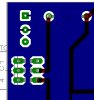
Well I tried to lay thermals down; selected polygon, switched on thermals in top row, named it gnd, clicked on ratsnest and copper pour worked. All components not named as gnd are isolated. However no sign of thermal pad.
The only way to do this manually is to then place a wire across from the pad to copper plane and name this gnd. Redo ratsnest and we now have a grounded pad - ideal for soldering.
Any other way of doing it would be appreciated.
Are you saying that pads connected to gnd in the schematic are not showing wiht thermals? Did you use the NAME tool, left click the polygon outline, and name it gnd?
If those things don't work and you are willing to send me both your sch and brd files, I will try it. Just attach it to a PM. John
Edit: Maybe this is a little clreaer. There are two times you have to name ground. Once in the command line with the polygon. Then you have to name the polygon by left clicking on it with the name tool.
Thanks John.
I'm not working directly with a schematic's autoroute function, only manual routing.
At last it works! - now I have VIA thermals on bottom layer.
You are right, naming polygon gnd in command line and clicking on it, name gnd
I started with clean board - no polygon - only vias and track.
TOP 1, BOTTOM 2, VIAS 18, tplace 21, torigins 23, names 25, tvalue 27, tdoc 51.
DRC - supply - tick generate thermals for VIAs....apply....select.
name all VIAs gnd.
polygon - select thermals in top tool bar to ON.
draw polygon - name in command line gnd and click on polygon, name gnd.
click on ratsnest.
view bottom layer to see thermals
This site uses cookies to help personalise content, tailor your experience and to keep you logged in if you register.
By continuing to use this site, you are consenting to our use of cookies.