Continue to Site

Welcome to our site!

Electro Tech is an online community (with over 170,000 members) who enjoy talking about and building electronic circuits, projects and gadgets. To participate you need to register. Registration is free. Click here to register now.

  • Welcome to our site! Electro Tech is an online community (with over 170,000 members) who enjoy talking about and building electronic circuits, projects and gadgets. To participate you need to register. Registration is free. Click here to register now.

XOR CIRCUIT

Status
Not open for further replies.

sxy

Member
When you press the right button,

How the second transistor from the left reaches the ON state.

After all, there is no closing of a circuit from the positive voltage of the voltage source, the current can not reach the negative voltage source, because it is stopped at the collector of the first transistor from the left,

When the first transistor is off.

So in my view the second transistor from the left, can not be turned on,

But actually it can.
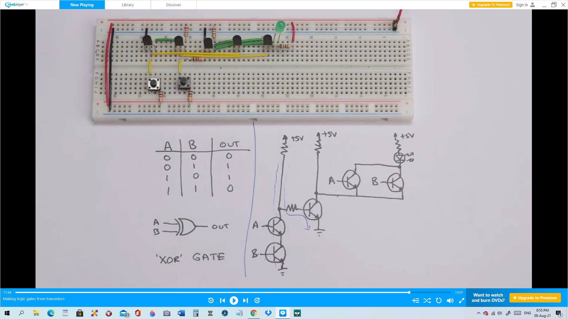
XOR CIRCUIT.png
 
which is the second transistor from the left? Could be one of three the way I look at it, add some labels please.
 
STOP SHOUTING.
Nothing is obvious,
As I said in the reply to your private message,
I only follow schematics, I've no idea of the pinouts of your transistors and no intention of trying to follow your breadboard layout.

Mike.
 
I UNDERSTAND THE SCHEMATIC
BUT I DON'T UNDERSTAND THE PICTURE
IN THE PICTURE IF YOU LOOK FROM THE LEFT SIDE
THE SECOND TRANSISTOR SHOUD NOT BE WORKING WHEN YOU PRESS THE RIGHT BUTTON
BUT ACTUALLY IS WORKING.
I DON'T UNDERSTAND WHY
 
2 MILLION VIEWS.
I don't care if it has a Zillion views.
That has nothing to do with your question.

Do as Pommie asks and post the schematic with transistor labels and the switches, if you want answers here.
 
No one here cares about a youtube video. Post a question with a schematic and we may be able to help.

Mike.
 
THERE IS A schematic IN THE QUESTION BUT I AM ASKING ABOUT THE PICTURE THAT IMPLEMENTS THE schematic .
 
THERE IS A schematic IN THE QUESTION BUT I AM ASKING ABOUT THE PICTURE THAT IMPLEMENTS THE schematic .
Sorry but we just want you say what you want from the circuit and what it actually does. Try it on breadboard and post what you did so far.
 
Please add reference designators to all components in the schematic and repost.

Also, indicate where the OUT signal is located.

ak
 
Last edited:
Status
Not open for further replies.

Latest threads

New Articles From Microcontroller Tips

Back
Top