Continue to Site

Welcome to our site!

Electro Tech is an online community (with over 170,000 members) who enjoy talking about and building electronic circuits, projects and gadgets. To participate you need to register. Registration is free. Click here to register now.

  • Welcome to our site! Electro Tech is an online community (with over 170,000 members) who enjoy talking about and building electronic circuits, projects and gadgets. To participate you need to register. Registration is free. Click here to register now.

Boost converter debugging

Howdy, first time poster. I'm a software engineer that's always enjoyed tinkering with electronics, and I'm working on a project to expand my skill set a little. An important part of this project is a boost converter to create 180V power for some nixie tubes. That's what I'm having trouble with right now.

I pieced together a design from various conflicting sources and calculators across the Internet. ;)

I bread-boarded a 5V to 12V version and that worked fine so I built a schematic, had a PCB printed and put it together.

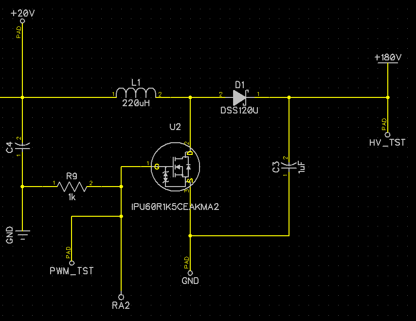
Here's the relevant portion of the schematic:
Screenshot 2023-12-23 200352.png


I've got a +20V power source, and I'm providing a 200kHz PWM signal from a PIC (that's the RA2 port at the bottom).

This is all kinda/sorta working. It's definitely boosting the voltage, but it's doing so in weird steps that I can't work with. At 25% duty cycle, it puts out about 80V and that climbs slowly as I increase the DC%. Around 30% it suddenly jumps from 90V to 145-165V and then levels off. At around 53% it jumps again to 230-240V! That's more than D1 is rated for, but it's hanging in there so far.

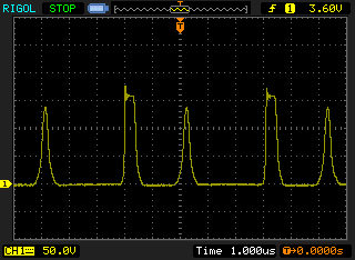
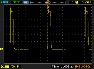
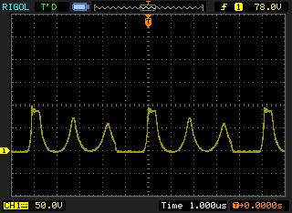
I hooked my oscilloscope up to MOSFET drain, and the waveform is weird. In the 25-35% duty cycle regime, there are three distinct peaks in the voltage every period. When it suddenly jumps to 145V, one of the peaks disappears. When it jumps again to 230V another peak disappears and I'm left with just one peak.

90V:
90V.png


145V:
165V.png


230V:
240V.png


The PWM signal isn't the cleanest, but I don't think it's the problem:
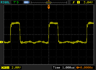
pwm.png


Any ideas on what's going on here?
 
You likely need a better gate drive circuit, to provide a higher voltage? It's barely switching on at 5V, it really needs more like 8V or so, and with enough current capability to drive the gate capacitance.

The bit of a dip at the leading edge of each pulse may be due to the gate-drain capacitance as it starts to conduct, forcing the gate voltage down.

You may also be getting some resonance effects as it switches with different pulse durations? With marginal drive, it may well switch erratically.

Are the input and output caps electrolytics? The schematic symbols indicate that? If so, add some ceramic or film caps in parallel as electrolytics are not good at high frequencies.
 
As already mentioned, you need better drive to start with, and you should run it closed loop, not open loop (which I presume is what you're testing it as at the moment).

I'm also a bit sceptical about such a high voltage increase from a simple boost converter, rather than a transformer based one.
 
When you try for such a high boost ratio you get a device that is hard to control. The slope of the output voltage to control voltage function is approaching the vertical. This means very small changes in duty cycle produce large changes in output voltage. A boost ratio of 4-5 is the top of what I would consider practical.

A good textbook on SMPS would do you a world of good. Here is a good one:
Basso, C., Switch Mode Power Supplies, 2014
 
Thanks for all the replies!

I was not suspecting the drive voltage was inadequate! Is that a property of the FET I could have seen from the datasheet? In other words, could I improve the situation with a more appropriate component choice? Having to boost the voltage from the microcontroller to the FET sounds annoying.

The caps are ceramic; that's just DipTrace gave me for 1206_CAP symbol. Sorry.

I am working up to closed loop control. I had a PID loop tuned for the breadboard version, I was just investigating the DC/V response before turning that on when I stumbled into this weirdness.

I hear y'all on 9x being an ambitious boost (and thanks for the book suggestion, Papabravo). I was already concerned about the relatively low resolution I have to tune my duty-cycle because of the higher frequency I'm running at. I only have 160 steps from 0% to 100%. I'm considering going with a larger inductor so I can lower the PWM frequency and get more resolution from my microcontroller.

Again, thanks for the replies. I've been having a blast with this project. Mostly figuratively.
 
Is that a property of the FET I could have seen from the datasheet?

Yes, have a look at diagram 7 on page 7 and diagram 9 on page 8 of the datasheet

With 5V gate drive on that device, the current limits to a low peak value and the "on" resistance is high.

The gate drive voltage should ideally be adequate to get it to its rated minimum "on" resistance, so around 8V or preferably 10V - that's where the kink vanishes in diagram 7.


Power MOSFETs also have quite high gate-source capacitance, sometimes several nanofarads, and usually need high current drivers when used for PWM, otherwise the turn-on and -off times can take a significant part of the switching cycle.

There is also significant capacitance between gate and source, which acts like negative feedback and opposes switching, if the gate driver cannot supply adequate current - I think that's what is causing the visible glitch down to 4V or so at the start of each gate pulse.
 
Awesome. I literally had diagram 9 up on the screen when the notification came through!

I hear y'all that this is really pushing what a boost converter can achieve, but I kinda just want to see if I can get it there!

So, bare minimum, I need to pick a MOSFET my microcontroller can actually drive.

I don't want to change too many other things at once. Does boosting the inductor size and lowering the PWM frequency sound like it will help?
I would also suggest you use a driver between PIC and FET, IC's are available, or discrete transistors - this is because the PIC can't provide enough current to switch the FET ON and OFF fast enough, resulting in it getting hot.

This driver uses an FET (for level shifting) and push/pull NPN/PNP drivers, I also tried 8 pin driver IC's, and this performed just as well. Without either of them, you could easily see the switching delays on the scope, and the FET got hot. This is actually a buck example (for boost take R13 to 0V instead of +ve), but my original test PCB included both buck and boost, with P-gate and N-gate FET's, using a single toroid, and was configurable as either, or both.

There are numerous examples on-line using Arduino's driving FET's directly, but this means they produce excessive heat.

Also don't try and run it open-loop, you need closed-loop if you want to try and get the voltage anywhere near what you want.

FET_Driver.png
 
So, bare minimum, I need to pick a MOSFET my microcontroller can actually drive.
PWM MOSFET driver circuits need to be able to source and sink at least 500mA in general, and for high capacitance FETs at high speed them may need to be rated at 2A or more.

A "bare" MCU pin can be used for simple low speed on-off switching with an appropriate FET type, but just do not consider it for high speed switching / PWM type applications, it will not work.
 
Also don't try and run it open-loop, you need closed-loop if you want to try and get the voltage anywhere near what you want.
I want to be sure I understand what you're saying here. In my line of work, "closed-loop" implies something like a PID function running in the microcontroller that adjusts the PWM duty-cycle based on measured voltage. Is that what you mean, or do you mean something in-circuit?
 
I want to be sure I understand what you're saying here. In my line of work, "closed-loop" implies something like a PID function running in the microcontroller that adjusts the PWM duty-cycle based on measured voltage. Is that what you mean, or do you mean something in-circuit?
Yes, that's exactly what I mean, the microcontroller monitors the voltage, and adjusts the PWM accordingly - PID would be good, but may not be required, depending on exactly what you're doing. In my case I'm charging Li-Ion cells, so it's not critical, and I don't bother with PID.
 
OK, good. I already have all the closed loop stuff ready to go. I'm getting a nice clean voltage reading at the microcontroller, and I have a couple control algorithms I've tested out on the bread board.

Thanks for everyone's help. I'm going to start filling in some knowledge gaps, do a redesign, and I'll report back on rev B once it's running!
 
While boost ratios of 10 are more difficult than smaller boost ratios, they are not impossible.

You do need some feedback. The PWM duty cycle doesn't control the voltage at all well if the current isn't flowing continuously in the inductor.

There has to be an average voltage across the inductor that is close to 0 V. So with a 20 V supply, and a 75% duty cycle, the average forward voltage is around 15 V, so the average reverse voltage also has to be 15 V, so that needs 60 V for the 25% of time remaining, so you get around 80 V. That works OKish when the current is flowing continuously.

However, if you have 20 V across a 220 μH inductor for 75% of a 200 kHz PWM signal, the current in the inductor will increase by 0.341 A, so if the current nearly gets to zero during the 25% off cycle, the average current will be 0.17 A, or around 100 times what you want.

What you will be aiming for is a circuit that occasionally turns on the MOSFET for a very short time, allows the current to build up to 10 - 20 mA, and then turns off. The inductor current will initially charge the output capacitor, and will then drop to zero for a longer period of time.

It could be that you need a larger value inductor.
 
You also have the issue of how much charge it takes to achieve the 180 V that you want. The charge needed will mainly be to charge up the capacitance within the MOSFET. However if you don't keep the MOSFET gate voltage low, the MOSFET will be conducting, taking charge from the inductor before the voltage gets up to the desired output voltage.

Any time that the voltage on the output side of inductor is above the 20 V input, the current in it will be reducing and there has to be some current left after the voltage gets to 180 V.

If you are using an open inductor, you may be able to add extra turns of enamelled wire to give more voltage.
 
I want to be sure I understand what you're saying here. In my line of work, "closed-loop" implies something like a PID function running in the microcontroller that adjusts the PWM duty-cycle based on measured voltage. Is that what you mean, or do you mean something in-circuit?
Most SMPS designers use a PI compensator.
 
Most SMPS designers use a PI compensator.
I'm thinking I can get away with just proportional control considering my load isn't very sensitive to the exact voltage. But I've got a PI algorithm already written for my PIC if I need it.

It could be that you need a larger value inductor.
I was playing around with adafruit's boost converter calculator and it was suggesting much larger inductors, 1-4 mH. I also want to drop the PWM frequency, which pushes me in the same direction. I don't remember why I used 220uH for this version, but it seems way too small.
 

Latest threads

New Articles From Microcontroller Tips

Back
Top