Continue to Site

Welcome to our site!

Electro Tech is an online community (with over 170,000 members) who enjoy talking about and building electronic circuits, projects and gadgets. To participate you need to register. Registration is free. Click here to register now.

  • Welcome to our site! Electro Tech is an online community (with over 170,000 members) who enjoy talking about and building electronic circuits, projects and gadgets. To participate you need to register. Registration is free. Click here to register now.

Check my PCB?

Status
Not open for further replies.

fouadalnoor

Member
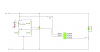
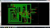
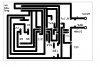
Hello guys, I'm trying to produce this PCB from the attached design, but I don't know if it would work.

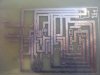
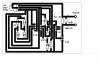
The one shown on the picture was made using a laser printer as shown in this video: https://www.youtube.com/watch?v=urv6jArKp6M

If you look closely you can see that some of the tracks slightly overlap and what do I do with the resistor "spaces" as they seem to connect to the track as well...

Any help appreciated!

Fouad.
 

Attachments

  • PCBReal.JPG
    PCBReal.JPG
    2.5 MB · Views: 159
  • PCBSchematic.jpg
    PCBSchematic.jpg
    322.8 KB · Views: 142
  • PCB-XPSImage.jpg
    PCB-XPSImage.jpg
    62.4 KB · Views: 145
hi,
A circuit diagram is required to check the actual artwork...;)
 
hi,
A circuit diagram is required to check the actual artwork...;)

Ah okay, its attached...(I dont have a proper schematic as it's a pretty simple project so its quite different from the actual PCB...)

The thing I just want to check is whether the layout of the pcb I posted above is correct to produce or should I change it?
 

Attachments

  • GasAlarm.png
    GasAlarm.png
    23.2 KB · Views: 139
Last edited:
The board you made looks good for a first attempt, other than the mistakes made.

Problem number 1 was you printed the silkscreen layer and is why you got the resistors and component outlines.........Dont do that!!
Just print the "Bottom layer" only.

Second problem is the smudging of the toner transfer joining the tracks together, it is always important to do a good visual check for problems before you etch.

Any problems can be removed with a small craft knife or scriber, by scratching away the bridges between the tracks to bare the copper before you etch.
Also if the holes are missing (as some of yours are) its a good practice to carefully scratch a small spot in the toner so a hole will etch, it dont need to be round or perfect just a small mark will do.
When you come to drilling this will make the job much easier, as without the hole in the copper the drill bit will be hard to locate in the correct spot and you are likely to break drill bits.

If you slip and remove toner that you should not have, then this can be repaired with a sharpie marker pen, or i used a CD label pen, just let the ink dry well before you etch.
Again if the pen ink gets where it should not have scrach it away before you etch.

It all might sound difficult, but you get rather good at it and quick with a little practice, and its a hell of a lot easier to fix the mistakes before you etch a board the afterwards.

Pete.
 
Status
Not open for further replies.

Latest threads

New Articles From Microcontroller Tips

Back
Top