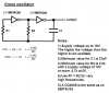
Continue to Site

Welcome to our site!

Electro Tech is an online community (with over 170,000 members) who enjoy talking about and building electronic circuits, projects and gadgets. To participate you need to register. Registration is free. Click here to register now.

  • Welcome to our site! Electro Tech is an online community (with over 170,000 members) who enjoy talking about and building electronic circuits, projects and gadgets. To participate you need to register. Registration is free. Click here to register now.

Help with circuit

Status
Not open for further replies.
Excuse me but sometimes it takes days for someone to respond, yet you get impatient after just 24 miniutes.

What do you mean by a mathematical explanation? The circuit is quite well explain in the text below the schematic.
 
The amplifier is a cmos inverter wirh negative feedback which biases its input at about half the supply voltage and makes it a linear amplifier. Its voltage gain is dependant on the supply voltage and on the ratio of the feedback resistor to the input resistors.
Its input impedance is low and its output impedance is high.

The bandpass filter is a simple highpass filter with C2 and a simple lowpass filter with C3.

The oscillator is a Classic Cmos Oscillator that is used everywhere.
 

Attachments

  • Cmos amp.PNG
    Cmos amp.PNG
    18.6 KB · Views: 141
  • Cmos oscillator.PNG
    Cmos oscillator.PNG
    23.2 KB · Views: 134
Excuse me but sometimes it takes days for someone to respond, yet you get impatient after just 24 miniutes.

What do you mean by a mathematical explanation? The circuit is quite well explain in the text below the schematic.

Thanks:) & I apoligize for being impatient.:eek:

I mean what are the mathematical expressions that govern the design of the amplifier and band-pass filter. For example, how did the designer arrive at those resistor & capacitor values. I'm asking this because i'm not familiar with a NOT gate used for this type of application. If you have a material that i can use to learn how to use them this way, i'll really appreciate it.

Thanks
 
I mean what are the mathematical expressions that govern the design of the amplifier and band-pass filter. For example, how did the designer arrive at those resistor & capacitor values.

By using a fan-dangled thing called a 'formula'... :rolleyes:

(Sorry my last couple of posts today have been rather scathing... It's 1am... =.=)

Check the attachments that Audioguru posted up.
If you have simulation software, I use multisim, a lot of the members here use pspice, draw up the circuit and see what effect it has when you change certain values...
 
Thanks for your response erosennin:),

I checked what Audioguru posted, what about the bandpass filter formula?
Apart from numerous simulations like using multisim (some of which didn't work) experimental,is there no theoretical way?

Thanks


By using a fan-dangled thing called a 'formula'... :rolleyes:

(Sorry my last couple of posts today have been rather scathing... It's 1am... =.=)

Check the attachments that Audioguru posted up.
If you have simulation software, I use multisim, a lot of the members here use pspice, draw up the circuit and see what effect it has when you change certain values...
 
It is almost impossible to acurately analyze this circuit, because CMOS inverters are digital devices, and are not characterized as analog amplifiers. You can generally say that the open loop gain of the 4049 will be fairly high, but with the high feedback ratio on IC1A, I would say it is impossible to mathematically predict the closed loop gain or bandwidth. Even a spice simulator would probably be wrong. You might be able to predict the response of the filter, if the transfer function turns out to be insensitive to IC1B's open loop transconductance and output impedance.
The rest of the circuit is pretty much digital.
Why do you want to analyze it? Just build the damned thing, and see if it works.:p
 
Thanks Roff for the quite detailed explanation.:)

It's not just to build it, actually, its so that i'll learn the theory behind what i'm doing.
To me, nothing's more humiliating than to actually do something without knowing what i'm doing, for example, if the circuit refuses to work, then i wouldn't know whether it's me or the circuit or whatever else; let alone to refine/improve on the design to my need.:eek:

That's why i want to learn the formulas. The description on the page sort of covers the operation, but how he did it is more important, atleast to have an idea of what's wrong when something goes wrong.:)

Thanks

It is almost impossible to acurately analyze this circuit, because CMOS inverters are digital devices, and are not characterized as analog amplifiers. You can generally say that the open loop gain of the 4049 will be fairly high, but with the high feedback ratio on IC1A, I would say it is impossible to mathematically predict the closed loop gain or bandwidth. Even a spice simulator would probably be wrong. You might be able to predict the response of the filter, if the transfer function turns out to be insensitive to IC1B's open loop transconductance and output impedance.
The rest of the circuit is pretty much digital.
Why do you want to analyze it? Just build the damned thing, and see if it works.:p
 
**broken link removed** is a link to an analysis of the bridged-T bandpass filter.
 
Status
Not open for further replies.

Latest threads

New Articles From Microcontroller Tips

Back
Top