Continue to Site

Welcome to our site!

Electro Tech is an online community (with over 170,000 members) who enjoy talking about and building electronic circuits, projects and gadgets. To participate you need to register. Registration is free. Click here to register now.

  • Welcome to our site! Electro Tech is an online community (with over 170,000 members) who enjoy talking about and building electronic circuits, projects and gadgets. To participate you need to register. Registration is free. Click here to register now.

Making a Bluetooth adapter for a Car Phone from the 90's

I found the source of the problem. The "speakerphone" IC (and a few other ICs) are not receiving any power supply at all. I traced the power supply track back to a small IC that I now assume is a 5V regulator, because the other pins on it are ground and constant 12V power (even when the car is turned off).
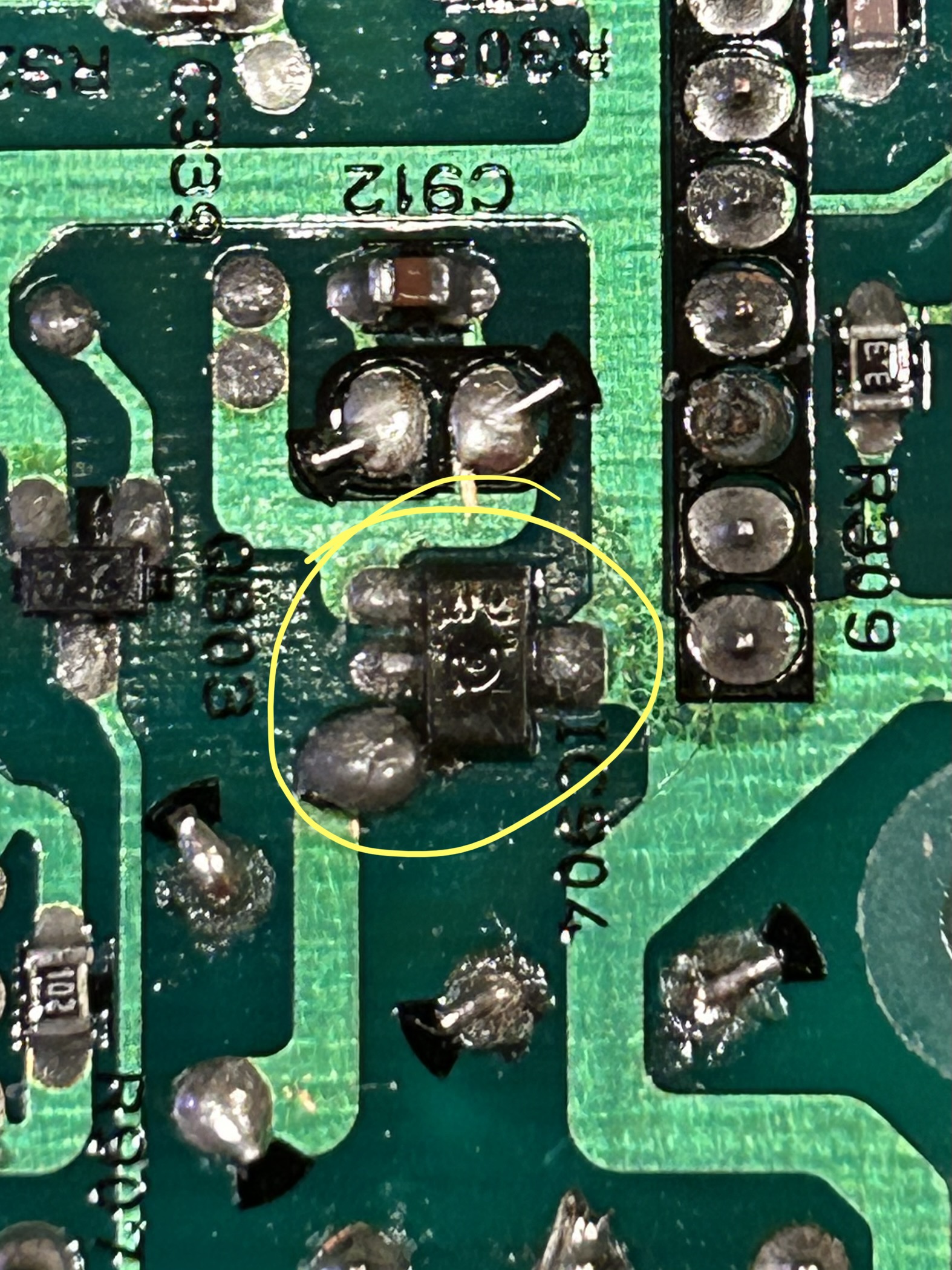

IMG_E2111.JPG

(everything is glossy due to conformal coating I sprayed on the board after cleaning and repairing)

The constant 12V input pin on this IC is one that was severely corroded by water damage previously, almost completely dissolved away. An electronics repair shop reconnected the small remaining stub of a pin with a solder bridge (giant blob). I suspect there was still some bad metal on that pin and the corrosion continued to spread and severed the repaired connection, or it just wasn't a good solder joint and it failed.

So good news: I'm pretty confident my new Bluetooth adapter design did not cause any problems.

Bad news: I'm not sure if I'll be able to save this.

I can't identify this IC. It has some faint markings on it. I think it may be "8606" or "8C06" or "8006". I could try replacing it with an arbitrary 5V regulator with the same footprint (3-Pin SOT-89?) and pinout that can handle ~12-14V input. Or maybe I could try removing the solder blob, scrape away a bit of the plastic case of the IC to expose more of the pin, clean it up, and repair the connection again with a piece of wire?
 
Looks like Vin and Vout are swapped on that component. In my photo, bottom is Vin, top is Vout, middle and right side is Gnd.

I found this L78L05ACUTR, which looks promising. The only spec I'm uncertain about is the max output current of 100 mA.

Before I order anything, I'll take a measurement of the output voltage on my remaining functioning module to confirm it is 5V, and also take a better look at all the components that receive power supply from this voltage regulator to see if 100 mA max seems reasonable. But the output voltage confirmation will have to wait a while because my remaining functioning module is in my car, which is still covered up for winter storage.
 
First, the good news: I have taken my car out of winter storage mode and tested my new design in the car with full hands-free integration, and everything seems to be working great! Its really nice to have the car phone installed exactly as originally intended without any additional external conversion devices/wires. It just works, looks all original, and can even be removed from the car and carried in portable mode as originally intended. No excuses and no compromises.

1713378346029.jpeg


The less good news: I have now put together a second converted car phone with the new custom PCBs, but have encountered a few issues of differences in performance/quality between the two. I need to identify the cause of these differences and figure out how to reliably avoid them before I can consider building more of these for sale:
  • One of the phones has more noise in the Bluetooth phone audio, similar to the noise I had with my breadboard prototype due to poor grounding (even the better phone has some of this noise that I was hoping would be eliminated by the custom PCBs with plenty of ground fill and via stitching).
    • By swapping parts between the two phones I have narrowed it down to primarily the Bluetooth module/daughterboard, but also the the custom cable that connects the Bluetooth daughterboard to the motherboard is contributing to some difference in audio noise.
    • I suspect the issue with the Bluetooth daughterboard may be inconsistent/poor solder joint quality on the ground pins of the BM62 bluetooth module. I did have issues hand-soldering these pins because the heat of the solder iron tip was quickly wicked away by the grounded shield on the BM62, resulting in ugly cold solder joints. I'm preparing to order a couple of these PCBs from JLCPCB with assembly of the side of the board containing the BM62 so I can test with good professional reflow soldered connections.
    • There was a bit of a learning curve when crimping terminals for my custom cable. I had a couple non-ideal crimps on the first cable I assembled that I thought I had fixed, but that cable causes a bit more audio noise than the second cable I assembled. I'll be ordering more terminals and rebuilding the first cable.
  • The second phone I assembled initially had a rapid clicking sound in all audio (including audio produced by the MCU; not just Bluetooth audio). I discovered this was caused by the power supply output of the Dayton Audio battery module lightly contacting a grounded part of the transceiver case (stupid oversight in how the module was positioned without sufficient insulation).
    • Solving the shorting problem immediately cleaned up the audio clicking. But then there was still sometimes some audio clicking.
    • I then discovered that the piece of foam I used to secure the battery module in place is actually somewhat conductive! So it was also partially shorting out random parts of the battery module and causing power supply fluctuations. The piece of foam I used in my first phone was different and not conductive at all.
    • I have solved all the shorting issues, but now that battery module is not fully charging the batteries. So I think I damaged the battery module.
    • Another battery module is already ordered, and I'll have to modify it and more carefully insulate/install it.

I also have been unhappy with the li-ion batteries I'm using because they are a bit too long to fit well in the AA battery holders (55mm length, compared to standard AA size of 50mm length). They need to be forced in, and they distort the shape of the holders. I have now learned that this is because I bought "protected" batteries, which have an over-charge/discharge circuit added to the negative end of the battery (increasing its length). The best unprotected batteries I can find that are actually the same length as standard AA batteries have about 10% less capacity than the protected batteries I'm using. I also learned that it's easy to remove the protection circuit and re-shrink-wrap the batteries (I already did this). I'll be testing/comparing the 1000 mAh unprotected batteries with the modified-to-be-unprotected 1100 mAh batteries to decide whether it's worth the hassle to modify the protected batteries for that extra 100 mAh capacity.

If I can solve all of these issues reliably, and assuming I don't encounter any new issues over the next couple months, then I think I'll have enough confidence to make a few more of these to sell. The proceeds would help recoup some of the money I've put into this project, and fund the cost of further development. I really want to develop a replacement for the Dayton Audio battery module that I can incorporate directly into my custom PCB design, because modifying that battery module to connect to my PCB is quite tedious.
 
Last edited:
Sounds good!

Note that if any one of the cells had a partial short, it may take a good few hours on charge for the power board balance circuit to equalise them - and with protected cells, it may not be able to do that at all, as the highest charge one may disconnect itself and confuse things.

I'd also advise soldering any miniature crimp terminals before folding the strain relief tabs over the insulation. The results with anything other than the manufacturers specific tooling can vary tremendously & generic tools often distort the contact, as well as not giving an ideal crimp.
 
Note that if any one of the cells had a partial short, it may take a good few hours on charge for the power board balance circuit to equalise them - and with protected cells, it may not be able to do that at all, as the highest charge one may disconnect itself and confuse things.

One of the 3 batteries test at a substantially lower voltage than the other two (3.4V vs 4.1V), so they are definitely out of balance. But I've switched to a different (new) set of unprotected batteries now anyway. With the new unprotected batteries and a new battery charging module, I'm able to achieve a full charge. And battery life is pretty good despite supposedly having about 10% less capacity (I got 19.5 hours of on/standby time and 6.25 hours of simulated moderate/heavy use). It's not worth continuing to modify the higher capacity protected batteries.

I do, however, still have a problem with battery charging. While monitoring current draw to know when charging is complete, I noticed some intermittent and large fluctuations in current draw. I think I've narrowed it down to unreliable contact between the battery holders and the batteries (touching the batteries and applying small amounts of pressure causes fluctuations in current draw). Sometimes the current draw will never drop down to a level that signifies that charging is complete unless I wiggle the batteries a few times.

The battery holders I'm using are pretty flimsy/flexible. I think I need to upgrade to something more sturdy with better contacts, which will require some slight changes to PCB layout for different footprints. I think I'm going to order some of these battery holders and hack them onto my current PCB to test them.

I'd also advise soldering any miniature crimp terminals before folding the strain relief tabs over the insulation. The results with anything other than the manufacturers specific tooling can vary tremendously & generic tools often distort the contact, as well as not giving an ideal crimp.

Are you suggesting that I ONLY solder the wire to terminal and not crimp it onto the wire at all (to avoid potential distorting the contact)? Only crimp the strain relief?
 
I use sidecutters or fine nose pliers to fold the contact area tabs firmly over the wire, then solder them. Then again with small pliers to tighten the strain relief section after soldering.

For the battery holders - try a trace of deoxit or just fine oil on the contacts?
 
Heya UselessPickles - I am working on a similar project, not nearly as extensive as yours, but I am wanting to use just the handset and a microphone and speaker through the corded cable. Ideally this would work with any car phone with an RJ connection, although I suspect there are differences of the wiring schematics. I am going to go though this thread again and see if you had gotten into the headset wiring, but do you have any tips or advice?

Basically, I would want to be able to plug a car phone headset into a landline and it hear dial tone and microphone works...
 
SwissBliss One of the earliest things I documented in this thread was reverse-engineering of the wired connection to the handset. I can't say for sure that this is 100% true for ALL car phone handsets, but I suspect they all follow a generally similar design as mine in that it requires some sort of serial data communication to control the handset and enable the speaker and microphone. Although you may get lucky and discover that your particular handset has an always-active speaker and microphone when power is supplied to the handset.

You will definitely not be able to connect a car phone handset to a landline and use it as a landline phone. Not only are the connectors incompatible (RJ45 vs RJ11), but the car phone handset is not a landline phone. The wiring is completely different.
 
I successfully repaired my spare Hands-Free Controller Unit with a new 5V regulator (L78L05ACUTR)!

1715056628272.png


Only slightly crooked :). The pad and trace leading to the 12V input to the regulator was quite damaged/missing, so I bypassed that trace with a wire.
 
After a long break, I'm back to working on this project. My latest prototype has been working reliably, so it's time to refine it some more. I want to quit relying on a modified off-the-shelf battery module (red board in this photo):

1733893382605.png


If I can design my own battery charging and power management circuitry, then I can eliminate several wires and connectors, and everything will be directly integrated on the PCB (no more loose circuit board held in place with foam, with risk of shifting and shorting out against something). This would also make it much more feasible for me to make several more of these conversions and sell them.

I spent several evenings researching battery charging/protection ICs. Some of my general findings were:
  • There do not seem to be any ICs that handle charging, protection, and cell balancing all in one. There are ICs dedicated to protection (some with additional cell balancing capabilities), some dedicated to balancing only, and other ICs that are dedicated to charging, and they need to be integrated together.
  • There are some protection ICs that handle only once cell, and can be chained together to protect/balance multi-cell packs, but there are also some protection ICs handle a range of multiple cells on one IC (some of which can also be chained together for even more cells in series).
  • Many charging ICs are pretty narrowly focused, such as:
    • Limited range of charging input voltage, primarily intended to charge via USB.
    • Requires the charging input voltage to be greater than the battery voltage (one example was a minimum of 2V higher).
    • Intended only for charging a battery pack that is disconnected and not powering anything (e.g., power tool battery chargers).
    • Some support being used in circuits where the device needs to be able to be powered while the battery is charging, but require substantial external circuitry to actually manage it (a.k.a., "power path management").
    • Some depend heavily on external components (e.g., external MOSFETs and driver circuitry), while others have more componentry directly integrated into the IC.
    • Some require an MCU to configure and control the battery charging, intended for more advanced systems like laptops that can monitor and optimize battery management.

Here's what I ended up finding that should work well for me:
  • Analog Devices MAX77960
    • Buck-boost charger that handles a wide range of input voltages and can charge the battery regardless of whether the input voltage is lower or higher than the battery voltage.
      • Automotive electrical system could supply anywhere from about 11.6V on a low nearly dead battery, engine not running, up to about 15V or higher with the engine running, which can be either below or above the 3-cell Li-Ion battery voltage.
    • Configurable through using configuration resistors on several pins to set other settings (completely standalone; no MCU control needed).
    • Built-in FETs (I only needed to add one external FET for inrush current protection when the protection circuit reconnects the battery).
    • Built-in power path management that can provide power to the system while charging, and can even do fancy stuff like throttling the charging to limit total current draw on external power in some situations, and even supplement external power supply with battery power in other situations.
    • Datasheet conveniently makes specific recommendations for a few important external components, and PCB layout for some of the most important components/traces.
  • TI BQ7791501
    • Single IC protects and balances 3 to 5 cells in series. Over/under voltage protection, and over/under temperature protection.
    • Configurable through a combination of selecting a specific part number with certain settings defaults as desired, and using configuration resistors on several pins to set other settings (completely standalone; no MCU control needed).
 
Last edited:
I'm now working with some pretty small components that would require custom breakout boards to adapt to a breadboard, and then probably wouldn't work properly in a breadboard anyway due to all the extra resistance and stray capacitance doing strange things I don't fully understand. So I'm going straight to a custom PCB and hoping I design the battery charging/management circuit properly (or good enough) the first time :)

Look at the footprint for the MAX77960:

1733896890489.png


And that's all crammed into a 4x4 mm IC. I'm not adapting that to a breadboard!

To minimize the cost risk of failure, I'm first designing a separate battery module that I can test separately, then plug into one of my existing car phone adapter motherboards (a replacement for the modified off-the-shelf battery module).

battery_module_3d.PNG


The 4 JST connectors are external power input, system power output, and two thermistors for temperature protection. The battery protection IC obviously uses a thermistor to disconnect the battery below/above certain temperatures. The charging IC also monitors temperature to prevent charging when too cold/hot (a bit redundant with the protection IC), but more usefully also reduces charging current at cold/hot temperatures that are not beyond the cut-off limits.

The "PWR" LED lights up when external power is supplied. The "CHG" LED will blink while charging, and light up steadily when charging is complete or near complete (all managed by the charging IC).

I'm making use of much smaller components than I've ever used before. I'm fully relying on JLCPCB to assemble all the SMD components, and completely abandoning the thought of keeping the design hand-solderable "just in case". This was necessary to come reasonably close to recommended PCB layouts for the ICS, and allowed me to pack everything together tightly enough that this entire board should fit in the same space where my modified off-the-shelf battery module currently sits in my project. The entire PCB is 60x93 mm.

If all goes well, I should be able to mostly transfer this entire PCB layout directly onto the motherboard for the car phone adapter, then make some small adjustments to eliminate JST connectors and directly connect the circuits together.
 
Last edited:
Here's a few screenshots of the PCB layout, zooming in on the most tightly packed area around the battery charging IC. I still probably have a couple evenings worth of double-checking my configuration of the two ICs, searching for all the parts on JLCPCB (trying to find as many resistors, capacitors, etc., as "basic" components to avoid parts loading fees), and cleaning up some traces and area fills in the PCB layout.

battery_module_pcb_layout.PNG


battery_module_pcb_layout_zoom1.PNG


battery_module_pcb_layout_zoom2.PNG
 
On the circuit schematic side of things, I learned how to properly make use of "hierarchical sheets" in KiCad to break the circuit apart into significant sub-circuits that can be connected together.

Here's the root sheet, showing the overall integration between the charging circuit, the protection circuit, the battery cell holders, and all of the connectors:

1733898449335.png


Here's the battery protection sub-circuit:

1733898862360.png


And finally the battery charger sub-circuit:

1733957931293.png


I'll definitely be taking what I've learned back to the schematics for the car phone adapter motherboard project to reorganize it better.
 
Last edited:
I think I'm just about done with this battery module circuit/PCB design.

I had to add a 5V regulator just to power two indicator LEDs. The only other sources of power were either not enough voltage to drive the LED, or too much voltage for the IC pin that is pulling low to control the LED.

I also cleaned up the board layout: packed some components tighter, widened the high current traces, cleaned up how some wide traces narrow down to connect to smaller pads, aligned some things to be more visually pleasing, improved labels for connectors and LEDs, and added important technical details to the back side.

I've identified specific JLCPCB part numbers for every part so that I can submit the design to them to build it for me. It's looking like it will cost about $140 to get two of these made/assembled/shipped, which already includes a $12-off coupon. About $66 of that is just fees for using "extended" parts. Maybe I'll make one more attempt to find "basic" alternatives to some parts. There are 5 parts not available in stock that I need to pre-order, and hope that JLCPCB doesn't run into trouble obtaining them.

Now I just need to sleep on it, then do one last review of the circuit design to double-check that I connected and configured everything correctly, cross my fingers, and start placing orders.

battery_module_3d_closeup.PNG


battery_module_3d_rear.PNG
 
(Warning: long post with multiple steps of my confusion before I reach a potential conclusion that I'm hoping someone can confirm is a good conclusion)

While doing some final review of my battery module circuit design, datasheets, etc., I have come to the realization that some of the features of the battery protection and battery charging IC and/or "typical application" recommendations are pretty specific to the assumption that there is a removable battery pack. I'm struggling to figure out how best to adapt this to my application where the battery pack is NOT removable.

Here's simplified circuit diagram focusing only on the relevant parts (you'll probably have to click/tap to enlarge and read the text):

1734398881129.png


Notes:
  • The Battery Protection IC and its related circuit all use -BATT as it ground, which is not always connected to the rest of the system ground (depending on current state of the various MOSFETS).
  • The Battery Protection IC CHG and DSG drivers output approximately the current battery voltage when "on".
  • Battery voltage will range from 8.4~12.45V.
  • The Battery Charging IC's SYS pin outputs either the battery voltage (when using battery power) or a steady buck-boost regulated 12.45V (when external power supply is connected; regardless of current battery level; possibly while charging the battery).
  • The Battery Protection IC has "load detection", and various faults won't recover unless load removal or load connection is detected (in addition to other relevant criteria, like the under-voltage condition is no longer present).
    • The LD pin is normally in an open-drain state.
    • After an under-voltage or any current fault, in addition to the relevant DSG and/or CHG drivers turning off, the LD pin is pulled down to -BATT through an internal 200k resistor.
    • The voltage at the pin is then monitored to detect whether a load is currently connected:
      • LD >= 1.3V: Load connected
      • LD < 1.3V: Load removed
    • If an external load is still connected, it has a connection to +BATT, but no connection to -BATT, except through the internal pull-down resistor on the LD pin (and external current-limiting resistor), and the external load will pull the pin voltage up.
    • Datasheet recommends increasing the R_GS_CHG resistor from 1M to 3.3M if load removal detection is needed for under-voltage recovery, because the CHG driver remains on during a UV fault (to allow charging), and that driver voltage output will be detected as load, even the battery pack is physically disconnected. The larger 3.3M resister divides down the voltage enough at the LDpin to fall under the threshold while no other load is connected.
      • But this is also not necessary if it's acceptable to require connecting to external power supply to recover from UV. When the charging IC starts charging the battery or using external power supply to provide SYS output power, there will no longer be a load on the battery.
  • The Battery Charging IC recommends an inrush current protection circuit (dashed box in the diagram)
    • Intended for when the battery pack is physically connected.
    • Inrush current is "absorbed" by charging up the capacitor and turning on the MOSFET before the system will be allowed to draw power from the battery.

So the problems/confusions I have found:
  • The "inrush current protection" circuit will always get enough voltage to keep the MOSFET on, even when the Battery Protection IC has disabled discharge, thanks to its connection to -BATT through the LD pin, and the values of resistors involved. So when the Battery Protection IC recovers and re-enables discharging, the "inrush current protection" won't protect against any inrush current.
  • The "inrush current protection" circuit also is enough load to pull the LD pin high enough to be detected as load, so the Battery Protection will ALWAYS detect that a load is connected.

I have played around with trying to calculate various resistor values to find a balance where:
  • The "inrush protection circuit" does not consume excess current (reducing its impedance is an easy way to reduce detected voltage at the LD pin).
  • The "inrush protection circuit" is guaranteed to both:
    • Turn its MOSFET on when discharging is enabled and the battery is at the lower end of its voltage range.
    • Turn off its MOSFET when discharging is disabled and the battery is at the upper end of its voltage range.
  • The "inrush protection circuit" is not detected as a "load"

But as I struggled with this, I started to think this may be overkill:
  • The MOSFET that enables discharging will already dampen the inrush current a bit, so maybe there's no need for the "inrush protection circuit"?
    • But will the MOSFET rise time be enough to dampen the inrush current enough?
    • I spent some time trying to find some simple formulas or online calculators to to help choose resistor values around the MOSFET to achieve a given rise time, but have mostly found complex theoretical stuff beyond my understanding, or very vague generalities.
  • I don't really need the load detection to fully "work". In fact, I think it would be best if the protection IC ALWAYS detects a load (the "battery pack" is technically permanently attached to a load):
    • Connecting to external power to charge the battery will be detected as "load removal" for the under-voltage condition.
    • None of the current-related faults should ever happen unless something is seriously wrong with the hardware. In that case, the problem needs to be investigated, so it is acceptable to require opening up the car phone and removing a battery to reset the protection IC. OTOH, it would probably be bad for the IC to detect "load removal" automatically after a current-related fault, because it could get stuck in a fast cycle of fault and reset, switching excess current repeatedly for hours/days, unattended in the trunk of my parked car. It's better to remain in a fault state until it can be investigated.

If I can't find any information to give me more certainty the next week or so, I think this is my plan:
  • Eliminate the seemingly useless "inrush current protection" circuit from my design.
  • Connect the LD pin to +BATT with the largest reasonable resistor value that will guarantee that the LD pin voltage stays above the load detection threshold at all times, even when the battery voltage is quite low, but also limiting current drained from the battery for load removal detection in under-voltage situations.
  • Switch to basic through-hole resistors for the charge/discharge enable MOSFET resistors so that I can easily experiment with different resistor values.
    • Start with stupid high values for MOSFET gate resistors like multiple MΩ? 10MΩ? I don't know what a reasonable starting point is. And start with a similarly high or higher gate-source resistor to ensure the gate voltage will be sufficient.
    • Use an oscilloscope to look at the inrush current when the discharge gate is enabled.
      • I'll be using potentiometers to simulate changes in thermistor readings, so I can trigger under/over temperature faults and recoveries to turn the gates on/off.
      • I can add test loops near the current-sensing shunt resistor so I can connect oscilloscope probes to catch the voltage spike across the resistor and calculate peak current from the peak voltage.
    • Through trial and error, decrease the resistor values until current rises very quickly, but without spiking too high.
 
  • Connect the LD pin to +BATT with the largest reasonable resistor value that will guarantee that the LD pin voltage stays above the load detection threshold at all times, even when the battery voltage is quite low, but also limiting current drained from the battery for load removal detection in under-voltage situations.
And this is why I shouldn't come up with plans late at night. This won't work. I need the protection IC to detect load removal when external power is supplied so that under-voltage faults can be recovered.

So I will need to connect the LD pin as originally intended. I think that should work fine. I can't even remember why I thought that was a good idea.
 
I removed the useless "battery inrush current protection" circuit, changed the charge/discharge MOSFET resistors to through-hole so I can easily experiment with different values, added several test points so I can measure voltage drop across the current sense resistor, and easily check voltages of the input, output, and the "protected" battery voltage seen by the charging IC.

I think I'm ready to send this in to JLCPCB to have it built, as soon as my pre-ordered parts are available.

1734495124732.png
 
While thinking about how to avoid excess inrush current from the battery whenever the battery protection IC enables discharging, I remembered that I have a bit of an ugly hack for MCU-controlled switched power that turns the phone "on" and "off", while allowing for a reboot that keeps everything powered in certain situations.

The negative side effects of my current solution are:
  • The switched power briefly turns on when battery power is first applied to the circuit while the MCU is initializing. This is generally annoying, "unprofessional"/glitchy looking, and could contribute to surge current when the battery protection IC enables discharging (because the handset will immediately begin drawing power).
  • There's a small amount of wasted power when the phone is "off", because the MCU is draining current through the pull-up resistor.

Here's a review of the current solution:

1735332066936.png


  • The pull-up resistor to +5V constant power generally keeps the load switches turned on unless the MCU explicitly pulls the MCU_SWITCHED_PWR_ENABLE pin low.
  • The MCU_SWITCHED_PWR_ENABLE pin will be in a high-Z state before initialization, which keeps power turned on during a reboot.
  • The MCU_SWITCHED_PWR_ENABLE is configured as an open drain IO pin, initially high, which continues to keep the power on during initialization.
  • Upon booting/initializing, my code decides whether to keep the power on, or turn it off (by setting MCU_SWITCHED_PWR_ENABLE low), depending on whether an EEPROM-stored value indicates that we are doing a special reboot with immediate power on.
  • To power off normally, I simply reboot the MCU (without setting the EEPROM-stored value to enable power-on after reboot), and the power will be turned off immediately after the reboot and initialization.
    • This simplifies power-on/off code, because it is always working from freshly initialized memory, etc., after a reboot, rather than needing to implement a lot of re-initialization code with risk of bugs that failed to properly re-initialize something.
  • To turn power on, I set MCU_SWITCHED_PWR_ENABLE high.


I have solved both issues with a very simple adjustment to the design!

1735332840229.png


  • The load switch now "latches" and keeps itself on through a pull-up resistor to the +5V switched output.
  • The overall MCU pin configuration and code is still the same, with only a slight code change to briefly change the pin from open drain to push/pull when I want to turn the switched power on.

So it's almost the same general solution, except that the switched power can never turn on until the MCU code explicitly turns it on because it is the switched power output that "holds" power on by default now. And the MCU no longer needs to continuously drain any power to hold a load switch pin low when power is turned off (I change the MCU pin back to high-Z when I put the MCU into sleep mode some amount of time after powering off).
 
After testing the adjustment to my power on/off circuitry and code on the breadboard (because I conveniently still have my partial breadboard prototype that I originally used to develop my power on/off circuitry and code), I made the same alteration to one of my PCBs for further testing, and it seems to be working as planned.

I removed the SMD resistor that pulled up to constant 5V, and soldered a through-hole resistor in its place, but pulling up to the nearest convenient switched 5V connection.

1735354734129.png
 

Latest threads

New Articles From Microcontroller Tips

Back
Top