electronium
Member
greeting fellow members of the forum
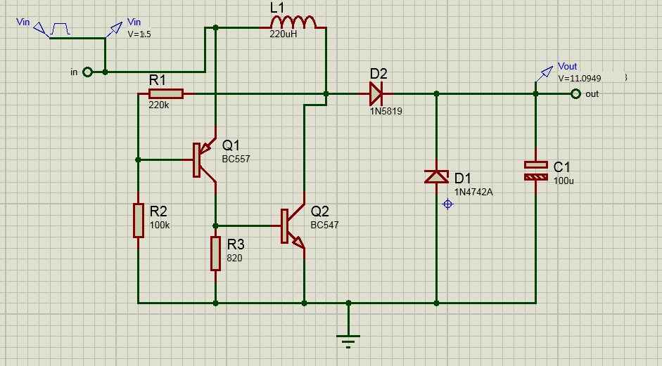
The voltage boost converter circuit was simulated and implemented with the help of friends. Now, if we want to use two bc547 transistors instead of bc557q1, what changes should be made in the circuit?
Circuit test and analysis video
Circuit schematic file
The voltage boost converter circuit was simulated and implemented with the help of friends. Now, if we want to use two bc547 transistors instead of bc557q1, what changes should be made in the circuit?
Circuit test and analysis video
Circuit schematic file
Last edited:

