Continue to Site

Welcome to our site!

Electro Tech is an online community (with over 170,000 members) who enjoy talking about and building electronic circuits, projects and gadgets. To participate you need to register. Registration is free. Click here to register now.

  • Welcome to our site! Electro Tech is an online community (with over 170,000 members) who enjoy talking about and building electronic circuits, projects and gadgets. To participate you need to register. Registration is free. Click here to register now.

Reduce PCB size

Status
Not open for further replies.
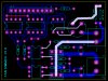
I've just realised another thing.

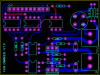
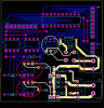
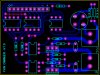
The PCB should be classified as reinforced insulation, so you should be able to run DC tracks over AC tracks on the other side of the PCB but you'll still need to keep 5mm clear of any component pins, vias and pads which have AC on them.

I normally wouldn't recommend this, unless you have no other choice.
 
The neutral is classed as the mains so yes, it needs to be at least 5mm away from the 5V.

The traces are made of copper which is not an insulator so how can that possibly help?

If you rotate the optocouplers circled in red clockwise by 90° and the one circled in cyan anti-clockwise by 90° it should make it easier for you.

The 47k resistors could bridge the mains traces where I've drawn a red rectangle, you'll obviously have to move the bridge rectifier, but it should be pretty simple.
 

Attachments

  • xxxxPCB.gif
    xxxxPCB.gif
    89.5 KB · Views: 140
No i meant like should 220 phase and Neutral be also away 5mm from each other?

Yes the trace will be from copper but i thought like maybe from Gauss's law or something the charge might be contained in and not flow out :D (just some guess work)

I have actually changed it a bit. Attached is the updated image.

The highlighted Traces are the Mains (220V) traces (boundry)
 

Attachments

  • Untitled-1.jpg
    Untitled-1.jpg
    238.2 KB · Views: 129
Oh no, the mains phase and neutral can be pretty close to each other, 1mm is fine, if I remember rightly.

I think you've missed the point about why there should be 5mm between the mains and 5V. The 5V side is a non-hazardous voltage which is safe to touch and will be connected to lots of potentially uninsulated metal parts. Therefore the insulation between the mains and the 5V side needs to be very good. This is because there can be some pretty high voltage spikes on the mains (>2kV) and it's important to protect the user from them. The insulation between the live and neutral is not so important because if it fails the user won't receive a shock, if there's a high voltage spike, it'll just arc over for a split second and nothing bad will happen, the worst case is the fuse will blow.

Your new board layout is much better. The only traces I'd be concerned about are the ones on the opto-coupler next to the bridge rectifier but if you CAD package says they're 5mm away from the 5V tracks then don't worry about it.

What size are you aiming for?

What size is it now?

You could probably make it a little smaller whilst still keeping to the 5mm rule.
 
59.8mm x 45.5mm are the new board dimensions. I think this is good enough. Actually user will not be touching any parts even from 5V section. It will all be controlled from a microcontroller using a Remote control. Actually some of the traces are 4.5mm apart but i think its still good enough.
 

Attachments

  • Untitled-1.jpg
    Untitled-1.jpg
    246.2 KB · Views: 130
Last edited:
I think the only 4.5mm dimension is on the top right hand opto-coupler next to the bridge rectifier.

Increasing it to >5mm is no problem, just shift the opto-coupler over a bit, see attached.

Now the circuit is safe to the point of passing the standards and small enough for you.
 

Attachments

  • mains PCB 5mm.png
    mains PCB 5mm.png
    16.8 KB · Views: 129
Last edited:
Of course you're right, silly me. :D

Here's a better idea.
 

Attachments

  • mains PCB 5mm.png
    mains PCB 5mm.png
    17.4 KB · Views: 128
Thank you, the orientation of PCB will seem random but i guess you are right (safety first than design). I will update my PCB to one you posted. :D

I've found a simpler solution: move the offending traces to the other side, see attached.

By the way I've been banned for two years after having a dissagreement with the moderator.

https://www.electro-tech-online.com/threads/i-dont-want-to-be-a-newby.107383/#post880080

I don't want to cause trouble but I wanted to post this attachemt.
 

Attachments

  • mains PCB 5mm use other side.png
    mains PCB 5mm use other side.png
    17.4 KB · Views: 149
Status
Not open for further replies.

Latest threads

Back
Top