Continue to Site

Welcome to our site!

Electro Tech is an online community (with over 170,000 members) who enjoy talking about and building electronic circuits, projects and gadgets. To participate you need to register. Registration is free. Click here to register now.

  • Welcome to our site! Electro Tech is an online community (with over 170,000 members) who enjoy talking about and building electronic circuits, projects and gadgets. To participate you need to register. Registration is free. Click here to register now.

Design simplification for PCB assembly - Need help.

ionBo

New Member
Hi!
First of all, since this is my first post, let me introduce myself. I'm Ben, 37yo, and English is not my first language so I will try to be as specific and precise as I can.

I have no particular knowledge in micro electronics, I try to learn as much as I can, but this time, I'm afraid I can't go further on my project without any help.

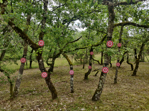
My project is a game I made for my kids who love to play indians, with their bow and sticky arrows. I made 10 targets (slaves), using arduinos, shock sensors, LEDs and NRF modules (and the master target with an added bluetooth module), that I spread througout the woods I have in my backyard. The kids run around, hit the targets and try to make the best score... The wireless design allows me to move the targets around and have them fairly spread out if I want to (up to 100 meters).

Here is how it looks, this picture was the first test I did with these (back in 2019), so I put them close together and just checked if everything was working correctly (I was fairly surprised when it did).
targetssetup.png


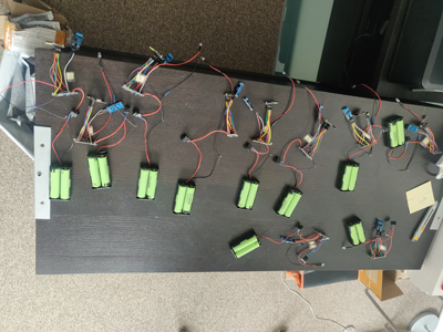
Here is my issue : I suck at soldering and this project took me weeks to assemble all the components. Also, the more the kids play with it, the more my targets "die" because a wire got loose and it is a real pain to find the issue and fix it. Yesterday, only 6 out of 10 were correctly working...

This is why I come to you with this question : how can I simplify my design as much as possible ?

My objective is to have as few components as necessary, and have a PCB made and all the components pre-assembled/soldered (or as many as possible), to reduce the possibility of poor soldering by myself, and save me time. A lot of time o_O
cablemess.png
cablemess2.png


Here are the components and the use I have of them :
- Arduino nano : it is just the brain, sending commands to other modules. I need a USB access to update the code if I need to.
- NRF24 - 2.4ghz radio module : used to communicate between slaves and master targets.
- SW420 - Shock sensor : detects a hit, sends a signal to the arduino that transmits the info to the NRF24 module
- LED - two colors, common cathode : lights green and red, depending on the game mode.
- JDY-31 - bluetooth module : only present on the master target, used to communicate with a PC (python) or Android (apk).

And this is the wiring :
A = Arduino
BT = JDY-31 BT module (Stat not used)
Shock = SW420 Shock Sensor
LED = Bicolor LED common Cathode
NRF = NRF24L01 (IRQ not used) - I have a 10uF capacitor added, as recommended in a few tutorials


A D6 ⇒ BT TX
A D7 ⇒ BT RX
A D5 ⇒ 220ohm resistor => LED 1
A D3 ⇒ 220ohm resistor => LED 2
A D4 ⇒ Schock DO
A D9 ⇒ NRF CE
A D10 ⇒ NRF CNS
A D11 ⇒ NRF MOSI
A D12 ⇒ NRF MISO
A D13 ⇒ NRF SCK
A 3.3V ⇒ NRF VCC + BT VCC
A 5V ⇒ Shock VCC
A VIN ⇒ Alim Positif
A Ground x2 ⇒ Alim Ground + BT Ground + NRF Ground + LED Ground + Shock Ground

I found tutorials on youtube showing how I could make a standalone arduino, using the chip and a few other components, but for the other modules, I have no idea how to proceed : their schematics are too complex for me and I don't know if I need all their components, for the basic use I have of them. I could maybe succeed with the shock sensor, it seems fairly simple, but I'm lost with the NRF and Bluetooth modules. I am also thinking of a possible improvement, by adding an external antenna to increase range and improve connectivity (trees are often blocking the RF signal, which is understandable considering the NRF module with its integrated antenna is stuck in a small project box, right next to other electronic components...)

Any help and advice with the design would be greatly appreciated!!

Thanks!
 
JimB : wow, thanks for the info! When I read your reply, I wanted to compare with other schematics for the shock module and found this one that I like because it adds a potentiometer that could be helpful to adjust the sensitivity

2748-Normally-closed-type-Vibrazione-Sensore-Modulo-alarm-Sensore-Modulo-Vibrazione-Pulsante-SW-420-arduino-compatibile.jpg


Is it any good ?


Also, I looked at the LM393 chip and...
ceLM393.jpg

Well, VCC and GND is easy enough. But I don't understand the rest. This chip is supposed to compare the normal voltage and send a signal when it detects a change.
Should I wire the vibration sensor to pins 2 and 2, and use the output 1 ? Is it that simple ?
No, the IC contains two comparators, you need to use one or the other - it doesn't matter which.
 
Well, VCC and GND is easy enough. But I don't understand the rest. This chip is supposed to compare the normal voltage and send a signal when it detects a change.
Should I wire the vibration sensor to pins 2 and 2, and use the output 1 ? Is it that simple ?
I get that you're trying to simplify as much as possible, but know that with these inexpensive modules, every fraction of a cent that can be engineered out already has been. If the designer could have left out a resistor or capacitor and the circuit still work, he would have.

What you are trying to do is not a trivial task and not likely to work on the first attempt. With JLC's assembly service (you won't find cheaper), you're paying for boards to be fabricated and 10 copies assembled....so you're paying for 10 sets of components and setup charges for parts not in their basic group.

I'm not trying to discourage you, just to set some realistic expectations.
 
I have started to sketch my circuit on EasyEDA and I am asking myself some questions. I could use some validation here, I read the datasheets and requirements but I'm still learning as I go and I might do something stupid with my components choices.

My input voltage is 7.4v (two 3.7v batteries in series) but the operating voltages are the following :
- ATMEGA328p : 5v
- NRF24 : 3.3v
- JDY-31 (BT module) : 3.3v
- SW420 (vibration switch) : the component is rated "up to 12v"

Therefore, I need a step down DC/DC converter, from 7.4v to 5v for the atmega. I found THIS ONE, seems about right ?

Now, on to the 3.3v elements : should I use only one step down DC/DC converter from 7.4v to 3.3v to power all the modules, or one converter per module ? Will only one module support the current drawn by the RF/BT an shock sensor ?
Would THIS ONE be a good choice ?

Thanks for your advice!

Edit
Nigel Goodwin : thank you for the precision! I makes sense :joyful:

For The Popcorn : I'm seeing that as well, when adding the different components to my board. However, I am ready to spend maybe 2$ more per board and have it sturdy enough to withstand rough handling and heavy things thrown at the targets. I don't want to have to change the modules plugged into the PCB every now and then, it would require having constant stock of these. Also, I like "neat things" and being proud of myself for doing this project all the way, and creating a functionning PCB from (almost) scratch.
 
Last edited:
I have started to sketch my circuit on EasyEDA and I am asking myself some questions. I could use some validation here, I read the datasheets and requirements but I'm still learning as I go and I might do something stupid with my components choices.

My input voltage is 7.4v (two 3.7v batteries in series) but the operating voltages are the following :
- ATMEGA328p : 5v
- NRF24 : 3.3v
- JDY-31 (BT module) : 3.3v
- SW420 (vibration switch) : the component is rated "up to 12v"

Therefore, I need a step down DC/DC converter, from 7.4v to 5v for the atmega. I found THIS ONE, seems about right ?

Now, on to the 3.3v elements : should I use only one step down DC/DC converter from 7.4v to 3.3v to power all the modules, or one converter per module ? Will only one module support the current drawn by the RF/BT an shock sensor ?
Would THIS ONE be a good choice ?

Thanks for your advice!

Edit
Nigel Goodwin : thank you for the precision! I makes sense :joyful:

For The Popcorn : I'm seeing that as well, when adding the different components to my board. However, I am ready to spend maybe 2$ more per board and have it sturdy enough to withstand rough handling and heavy things thrown at the targets. I don't want to have to change the modules plugged into the PCB every now and then, it would require having constant stock of these. Also, I like "neat things" and being proud of myself for doing this project all the way, and creating a functioning PCB from (almost) scratch.
You don't need to plug the modules in, you could solder them in, and it would be just as strong as soldering components directly to the board - or you could plug them in, and apply a little hot melt glue over the plug/socket seam, to prevent them coming loose.

The problem really is that the modules are so stupidly cheap, and avoids the difficulties of messing with SM components, which take a LOT longer to assemble than through hole ones. I generally use SM only where there's no option - I ordered some PCB's yesterday, which is all through hole apart from two components. If tiny size is important, then SM is the way to go - otherwise stick to through hole.

I appreciate your desire to create the entire design from scratch, but it's probably going to cost you considerably more to do so - and you're also probably not going to be able to build your own versions of all the modules.

As a minimum 'easy' option, just replace the nano - it's easy to stick a processor on the board, and you can buy through hole versions, complete with the boot loader ready installed
 
Nigel Goodwin : I had a PCB made specifically for soldering the modules (please don't pay attention to the track width... but hey, it does work)

pcb.png


But I gave up after soldering all the components to just one of these. Takes too much time to do it all, and I am definitely not good enough at soldering to make these correctly...

I had thought of a second version :
pcb2.png

I could order these with the connectors already soldered, and all I would have to do is plug the modules (the SW-420 socket is there, and in JLCPCB parts, just not 3D rendered). However, with all the modules in place, everything is really tight and I know from the previous PCB that the modules dimensions are slightly larger than what they are on the software. This design takes that into account, but there is a possibility it won't fit inside my project box (7.5x4.4cm).

I have listened to the comments posted previously : I am going to forget about putting the RF and BT components directly into the PCB. I will keep them as separate modules, plugged/soldered into the final PCB.

Also, I wish I could place the vibration switch (SW-420) directly into the PCB but JLCPCB and LCSC don't have the reference in stock (not even as a listed part...), so it looks like I'm stuck with the module, unless I build the courage to order the part separately and solder it myself on the final PCB.
 
For the atmega, I think I will use a socket already soldered to the pcb, and use a specific arduino uno shield (see picture below) to flash the chips (load the bootlader, then the code). I think it's the fastest way to program the atmegas as fast as possible...

shield.png
 
A couple comments:

Regarding the AP63205 buck converter – I would be concerned if the battery voltage will reliably power the 5 volt converter. I didn't see anything about dropout voltage/overhead voltage in a quick scan of the datasheet. Others will have more knowledge about this than I do.

Regarding the 5 volt supply in general – the ATMEGA chip looks like it's happy at 3 volts. Do you even need 5 volts?

And a bonus question: Are you including battery discharge protection on the board? Some LiIon batteries have it built-in, some do not. LiIon batteries express their displeasure at being over-discjarged by bursting into flames.

Sorry if any of this is redundant.
 
A couple comments:

Regarding the AP63205 buck converter – I would be concerned if the battery voltage will reliably power the 5 volt converter. I didn't see anything about dropout voltage/overhead voltage in a quick scan of the datasheet. Others will have more knowledge about this than I do.

Regarding the 5 volt supply in general – the ATMEGA chip looks like it's happy at 3 volts. Do you even need 5 volts?

You get different versions of the boards, the 3.3V ones only run at a slower clock speed - 5V boards are 16MHz and 3.3V are 8MHz (8Mhz should be fine anyway). As far as I'm aware the chips are the same, but it's a speed/voltage limitation of the processor.

The buck converter would be fine fed from two Li-Ion in series, personally (if I wanted 5V) I'd use one Li-Ion (or more in parallel) and a boost converter to give 5V.

If everything is 3.3V compatible, then choice an 8Mhz clock speed, and run it all at 3.3V - it makes life simpler, and an LDO 3.3V regulator is all that's needed. I like the MicroChip MCP1700-3302 regulator, which is 250mA, very low drop out, and very low quiescent current.

And a bonus question: Are you including battery discharge protection on the board? Some LiIon batteries have it built-in, some do not. LiIon batteries express their displeasure at being over-discharged by bursting into flames.

Not quite, they tend to catch on fire if over-charged, over-discharging just ruins them.
 
For The Popcorn and Nigel Goodwin : yes, you're right, the Atmega328p seems ok with 3.3v.

Taken from the ATMEGA328p datasheet (same specs for the 28dip or the square flat version):
2.7V to 5.5V for ATmega328P
0 to 8MHz at 2.7 to 5.5V
0 to 16MHz at 4.5 to 5.5V

Since it is very inexpensive and has quite similar specs to the MCP1700-3302, I think I will use the XC6206-3.3v. Please hit me on the back of the head if I'm doing something stupid :happy:

If I run the chip at 3.3v, I guess I will have to change the crystal, from a 16MHz one to 8MHz. Am I correct ?

I had not thought of going 3.3v all the way. I kind of stayed with the old "energy" design, since the Arduino needed 5v to operate...

With 3.3v, I can go with a single Li-Ion 18650 battery (3.7v, 3400mAh) and still have a decent operating lifetime. Correct me if I'm wrong but adding all the operating currents of the components should give me the current "consumption" per hour ?
Atmega : 0.2mA
JDY31 : 7.3mA
NRF24 : 20mA
SW420 : 15mA

If I round it up at 50mA (with the other components), is that a good guess ? Does it mean that with a single 3400mAh battery, I will get more than 60 hours of battery life ?
 
For The Popcorn and Nigel Goodwin : yes, you're right, the Atmega328p seems ok with 3.3v.

Taken from the ATMEGA328p datasheet (same specs for the 28dip or the square flat version):
2.7V to 5.5V for ATmega328P
0 to 8MHz at 2.7 to 5.5V
0 to 16MHz at 4.5 to 5.5V

Since it is very inexpensive and has quite similar specs to the MCP1700-3302, I think I will use the XC6206-3.3v. Please hit me on the back of the head if I'm doing something stupid :happy:

Never heard of it, but it's not critical or anything.

If I run the chip at 3.3v, I guess I will have to change the crystal, from a 16MHz one to 8MHz. Am I correct ?

Yes, just change the crystal for 8MHz - here are examples of the Arduio Pro Mini:


And here's a nice explanation:


I had not thought of going 3.3v all the way. I kind of stayed with the old "energy" design, since the Arduino needed 5v to operate...

With 3.3v, I can go with a single Li-Ion 18650 battery (3.7v, 3400mAh) and still have a decent operating lifetime. Correct me if I'm wrong but adding all the operating currents of the components should give me the current "consumption" per hour ?
Atmega : 0.2mA
JDY31 : 7.3mA
NRF24 : 20mA
SW420 : 15mA

If I round it up at 50mA (with the other components), is that a good guess ? Does it mean that with a single 3400mAh battery, I will get more than 60 hours of battery life ?

Yes, should last fairly well - bear in mind an 18650 is 4.2V fully charged.
 
So, I've made two different schematics on EasyEDA, turned them into PCBs, did a quick routing trial and sent the files to JLCPCB to have an idea of the cost difference...

Hare are the results (please don't mind the messy schematics, I'm still learning, and the design is far from perfect)

1 - All elements are modules plugged on female/male headers or connectors
allmodules.png


The PCB itself (15 pieces order) : 2.8€.
The PCB with all the modules : 9.6€

2. Only the RF and BT modules remain, the shock sensor is on the board, as well as a socket for an ATMEGA328p DIP28, and the board runs on 3.3v
atmega3v.png


The PCB itself (15 pieces order) : 4.7€
The PCB with all the modules : 11€

However, with the second option, my grand total for the project is lower than with the first version. The difference is in the reduced cost for the batteries... I only need one instead of two, to run 3.3V, also making the unit a bit lighter.

I would like to try option 2 and order some PCBs... Question is : will it work ? I followed the schematics for the "standalone arduino", for the shock sensor and for the voltage regulator but... I'm far from being an expert.

Any advice or comment on the second schematic (are there mistakes ? room for improvement ?) is welcome !
 
I think if we take it slow and break it down into smaller parts, it might feel less daunting. And maybe we can try to keep things as simple as possible? Like, not adding any extra stuff we don't need. Also, if there are any ready-made pieces or designs out there that we can use, that would be awesome. And I'm open to getting some help or tips from folks who've been through this before. Let's just take it one step at a time and keep it organized. With a little bit of guidance, I think we can make this project way more manageable.
 
To help with your reliability issues, use hot glue or silicone for strain relief on wires and loose parts.
  • Use resin flux jar to dip wires works better than just flux-core 1mm solder wire.
  • clean board of any oxide with a light 600 grit pre-scrub, if hard to solder.
  • Always keep the solder tip clean with a wet sponge , coated with solder
  • Don't use fixed power irons that are too hot, if so make a dimmer switch box at 75% or whatever works best.
  • A 1/16" tip works better and then the solder should flow towards the heat in < 1 second then release quickly.
  • pre-tin wires and pads before attachment then they bond easier
  • secure with hot glue, silicone or sub-floor PU adhesive. Wire solder joints will break otherwise.
  • Use loops or a magnifying glass stand to view solder better.
  • 1711090044415.png

1711088720633.png I would just use a < $1 electret Mic with pullup R to control gain ( Bigger R, more gain) and diode rectify with filter cap into a logic level pulse.
 
Attention!

Year old zombie thread, re-animated by a time waster.

JimB
 

New Articles From Microcontroller Tips

Back
Top