Continue to Site

Welcome to our site!

Electro Tech is an online community (with over 170,000 members) who enjoy talking about and building electronic circuits, projects and gadgets. To participate you need to register. Registration is free. Click here to register now.

  • Welcome to our site! Electro Tech is an online community (with over 170,000 members) who enjoy talking about and building electronic circuits, projects and gadgets. To participate you need to register. Registration is free. Click here to register now.

fabrication of a transistor

Status
Not open for further replies.

4electros

New Member
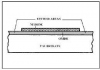
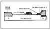
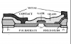
This is the basic fabrication sequence of fabrication NMONS transistor at SGS-THOMSON.
I also have details about the process stages but I wonder whether anyone here have any clue cause i couldn't understand it very well.

thanks in advance!
 

Attachments

  • 1.PNG
    1.PNG
    15.4 KB · Views: 141
  • 2.PNG
    2.PNG
    4.4 KB · Views: 159
  • 3.PNG
    3.PNG
    4.7 KB · Views: 140
  • 4.PNG
    4.PNG
    5.9 KB · Views: 147
what is there to understand there is wafer with either PNP or NPN material which is doped and enclosed in glass with a lead connection out. the doping is the gate or base or whatever.
 
Perhaps this link may help..
**broken link removed**

Mr Friedrichs puts theory into practice and makes his own thermionic devices ( vacuum tubes ) but has on occasion made his own transistors all wonderfully documented in his books, he also describes a posibble method for home contruction of FET's and more interestingly a brief reference to the work of Robert Pohl and Rudolph Hilsch and the experiments using whole crystals as a semicondutor without the need for complex doping or contruction methods.
 
Status
Not open for further replies.

Latest threads

New Articles From Microcontroller Tips

Back
Top