Electro Tech is an online community (with over 170,000 members) who enjoy talking about and building electronic circuits, projects and gadgets. To participate you need to register. Registration is free. Click here to register now.
Welcome to our site! Electro Tech is an online community (with over 170,000 members) who enjoy talking about and building electronic circuits, projects and gadgets. To participate you need to register. Registration is free. Click here to register now.
No need for information, just make up a bunch of stuff.
You are asking for a four-output boost converter. That is a significant design task, and a lot to ask for for free. What have you done so far? P;ease post your schematic / block diagram / whatever.
What is this for? What is the load current for each of the four outputs? How much current is available from the 0.7 V power source?
The "Joule thief" type circuit stores a small amount of power over time then discharges it in a brief burst, then repeats; it is not a continuous output & there is no more energy output than input.
"Power" is energy x time.
Critical points:
You do not get anything free in physics / electronics: Power out = Power in (as both wanted output and circuit losses); that's basic "Conservation of Energy"; TANSTAAFL.
For a 5V output from 0.7V, the current at 0.7V will be something over seven times higher than current at the 5V output.
Current * voltage IN = current * voltage OUT; not counting losses (which are quite high when starting with very low voltage).
So eg. if you wanted 1A at 5V continuously, the input current would be well over 7A continuously at the 0.7V input.
Without having you learn the basics of boost converter design, giving you a circuit would be malpractice, since you would try to build it on a breadboard which you should not do, and you would have little to no clue how to debug it if it did not work. Worse would be trying to layout a PC board without the knowledge of how to do it correctly. You will be much better off buying what you need or close to it to get what you need and maybe learn from it.
If you want to learn the basics and want to experiment safely, I highly recommend the use of a simulator and appropriate online textbooks.
I'm sorry, sir, I'm not a student of this major, and I have never learned the knowledge of switching power supply. The purpose of my question is to know the idea of circuit structure, and then find suitable materials to learn to build the circuit.
Thank you so much! I've been struggling with this for the past few days, but nothing has progressed, and your reply really points me in the right direction. Thank you very much!
ETA: The original question in this thread was about "Boost Converters". The simulation example is about a DC to AC inverter. The reason for showing this example was that it facilitated my own understanding of the operation of this variation of SMPS (Switched Mode Power Supplies). The book by Hart covers this variation as well as the Boost DC-DC converter.
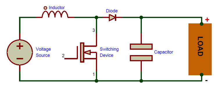
The basic "Boost converter" is extremely simple in principle - in fact the operation is very similar to a "ram pump" for lifting water, dating back to the late 1700s!
The switch is closed for a brief time for current to build up in the inductor. When the switch opens, the current continues to flow as the stored energy (magnetic field) in the inductor discharges.
That current passes through the diode and in to the storage capacitor and load.
Output regulation is by controlling how long the switch is closed (so how much the current builds up) during each switching cycle.
Ram pump -
The "inductance is water inertia in the inlet pipe at 1.
The "switch" is the weighted valve 4, which closes when the water flow is great enough to lift it so it blocks.
The one way valve at 5 is the diode, the accumulator 6 is the output storage & 3 is to the "load" - whatever uses the water.
This site uses cookies to help personalise content, tailor your experience and to keep you logged in if you register.
By continuing to use this site, you are consenting to our use of cookies.