mstechca
New Member
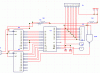
Take a look at this circuit.
The 1's in the boxes are output connections. the bottom "1", if it is logic high indicates that the last address has passed.
The top "1" is a check bit. It makes sure that the LSB is correct.
Connection "1" on the far left activates the address clock upon reaching a logic low.
Connection "2" on the far left resets the address clock upon reaching a logic high.
The numbers 1 through 8 (not sequentially) going downwards on the right hand side indicate the data pins on the parallel port.
Here's the problem. As soon as the circuit is turned on with 5VDC, and the parallel port is plugged in, the ROM chip immediately warms up.
Every time the chip warms up, the programming normally fails.
The chip that warms up is the 28C64.
The other chips are the 74HC00 NAND, and 2 4040's.
The other resistors are 6.2K.
Should I remove a resistor or increase a resistor?