Electro Tech is an online community (with over 170,000 members) who enjoy talking about and building electronic circuits, projects and gadgets. To participate you need to register. Registration is free. Click here to register now.
Welcome to our site! Electro Tech is an online community (with over 170,000 members) who enjoy talking about and building electronic circuits, projects and gadgets. To participate you need to register. Registration is free. Click here to register now.
hi,
D3 is a 5.6V Zener
Ignore the Ip, 0.01, they are for simulation only.
Use a JFET CC, is a junction FET Constant Current sink
The .dc V2 etc...... is a simulation command, ignore it.
hi,
D3 is a 5.6V Zener
Ignore the Ip, 0.01, they are for simulation only.
Use a JFET CC, is a junction FET Constant Current sink
The .dc V2 etc...... is a simulation command, ignore it.
Alec-t asked if it would be possible to simply use a POT immediately after the COIL around the first Opamp, then set the range between the two different circuits (1mv-1 and 1-10) each time.
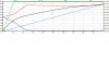
In this early question of yours, you ask if I want linear? I was wondering if there is a way of adding components that give a none linear line, as my black line on your Graph (attached).
This would be a luxury, failing this, I'm more than happy with your original design.
This site uses cookies to help personalise content, tailor your experience and to keep you logged in if you register.
By continuing to use this site, you are consenting to our use of cookies.