Continue to Site

Welcome to our site!

Electro Tech is an online community (with over 170,000 members) who enjoy talking about and building electronic circuits, projects and gadgets. To participate you need to register. Registration is free. Click here to register now.

  • Welcome to our site! Electro Tech is an online community (with over 170,000 members) who enjoy talking about and building electronic circuits, projects and gadgets. To participate you need to register. Registration is free. Click here to register now.

Mosfets drain (n type the tab on to-220 mosfets)

MrDEB

Well-Known Member
I want to attach all 8 tabs to the circuit board as heat sink but can I attach all 8 on together on the circuit board?
 
Your mounting hole looks too close to the pins by my calculations. But I just made post #69 for my own benefit
 
Last edited:
I MEASURED AND COME UP WITH 13.5mm but I need to reconfirm.
My issue now is I exceeded 300 connections so some of the heat pads won't get as many vias or look at redoing in EASYEDA?
 
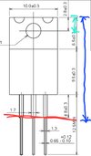
The picture shows the dimensions for the TO-220 package. The red line shows where the leads should be bent.

The blue line shows the length of the package from bend line to the end of the tab:

6.5 + 9.5 + 4.8 = :20.8 mm

The green line is the distance from the edge of the tab to the center of the mounting hole, so distance between pins and mounting hole equals

20.8 – 2.8 = 18mm

I showed 17mm in my drawing in post #69, which would be slightly tight but ok with the tolerances.

From your post, the distance between pins and mounting hole looks to be about 13mm, about ¼" shorter.

Screenshot_20240330_065349_Edge.jpg
 
I know popcorn uses EASYEDA and after drawing a schematic and PCboard using EASYEDA I am wondering if using the "solid area" function will produce the thermal pads for my MOSFETs?
 
If you follow my suggestion above, and create a footprint once, you'll use "solid region". This is simple because placing vias doesn't require that you assign them to a net.

^^^ This sentence only applies to creating a footprint as defined in post #69.

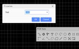
EasyEDA copper area in footprint.jpg


If you insist on being a masochist and want to "add it on" to a circuit board (which requires duplicating effort many times) , you'll need to use "copper area" to define the regions. This requires defining which net the region is connected to, which will be the drain of the MOSFET and different every time. You'll have to define the net for the stitching vias too. Hint - place the first via, edit the net property, and copy&paste it repeatedly. Hint - set the grid spacing to the spacing you want for the vias. Maybe 1 or 2mm.

EasyEDA solid region in pcb.jpg

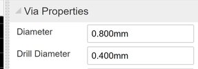
Use the via tool to create vias. Suggestion - there's no need to press the limits of the fab house. There's no need to go smaller than a 0.4mm drill with a 0.8 annular ring, Hint - set the properties on the FIRST one before copy&pasting, Then you only have to do it once.


EasyEDA Via properties.jpg


Perhaps, if you've found this advice and help, or any help I've given you in the past decade valuable, you could make a donation to the West Seattle Tool Library? A tax-deductable donation goes towards their mission of lending tools to the community at little or no cost.

 
I know popcorn uses EASYEDA and after drawing a schematic and PCboard using EASYEDA I am wondering if using the "solid area" function will produce the thermal pads for my MOSFETs?
The MOSFETS you are using have very low on-resistance. Are you sure such complexities of heat management are needed for a 3-amp load when these are rated for dozens of amps? Also, you can cut the heat of each one by half by simply putting two Mosfets in parallel. - which can be cheaper than the extra board space of laying them flat (which isn't always the best way to dissipate heat from the TO220 tab if you don't have a lot of copper space on the board surface. The PCB is acting like a blanket on the back side of the tab when you have only your small copper pad. Leaving them standing straight off the board means you'll get more convective air flow. So many thoughts and not enough experimentation and data.
 
Are you sure such complexities of heat management are needed for a 3-amp load when these are rated for dozens of amps?

This has been stated numerous times in the first THREE pages of this thread and been ignored.

The question of how hot the MOSFETs get has been asked several times. The only answer we've received is:

I want to AVOID ANY HEAT. HERE IS MY PRELIMINARY BOARD .

I don't see how the board can work at absolute zero, since electrons stop moving, but I'm sure I don't know everything.

MrDEB is going to do what MrDEB does, and read into answers whatever he wants to see.
 
PS, I'm not advocating MrDEB add heatsink areas; I'm just trying to show him how to do it without building scrap boards. So I don't understand the need to quote MrDEB's message mentioning me, which has nothing to do with your comment.
 
Thank you very much for making a donation. It's very appreciated. WSTL has a great mission of helping the community by making available all kinds of tools from lawn mowers to socket sets to table saws and DVMs. They also have a small workshop space with a large panel table saw, table routers, miter saw, planner, joiner, wood lathe, metal lathe and a large-format laser-cutter.
 
The MOSFETS you are using have very low on-resistance. Are you sure such complexities of heat management are needed for a 3-amp load when these are rated for dozens of amps? Also, you can cut the heat of each one by half by simply putting two Mosfets in parallel. - which can be cheaper than the extra board space of laying them flat (which isn't always the best way to dissipate heat from the TO220 tab if you don't have a lot of copper space on the board surface. The PCB is acting like a blanket on the back side of the tab when you have only your small copper pad. Leaving them standing straight off the board means you'll get more convective air flow. So many thoughts and not enough experimentation and data.

Agreed. The IRLZ44 will barely feel warm to the touch without a heat sink at 3 Amps.
 
Agreed. The IRLZ44 will barely feel warm to the touch without a heat sink at 3 Amps.

This has already been pointed out numerous times in the first 3 pages of the thread. No need to clutter the thread stating the obvious again.
 
This has already been pointed out numerous times in the first 3 pages of the thread. No need to clutter the thread stating the obvious again.
Then why clutter the thread for instructions how to solve a non-existent problem - no need to describe how to draw a heat sink and creat thermal vias
 
reason for the heat sink pads is for insurance to keep the temperature down as the PCboard is to be enclosed in a covered enclosure with an open grill-covered area for ANY heat.
I realize this may be over kill but better now than later.
 
reason for the heat sink pads is for insurance to keep the temperature down as the PCboard is to be enclosed in a covered enclosure with an open grill-covered area for ANY heat.
I realize this may be over kill but better now than later.
You can look up the dissipation of a black box and thickness of the plastic and type of plastic. Even when totally enclosed, the ambient temp will not rise much at all for a board the size you have and, at steady state, will make no difference if the mosfet is mounted to PCB to dissipate heat or is in free air inside the box. The heat has to get through the walls of the box either way. Convection of air around the TO220 tab will be better when they are off of the PCB when the whole thing is in a sealed enclosure. Then the warm air can circulate to the enclosure walls and dissipate to the surroundings.
 
The arguments against the need to use the board for heatsinking have been made in the first three pages of this thread. And rejected by MrDEB. This is his decision.

Discussed and rejected.

So the issue is helping him with what he wants to do.
 
Hi all...at the risk of getting hit by a passing arrow....:)

I think the focus should be elseware. For example, why voltage followers? Why multiple PWM generators? Why voltage divider at gates? What is dissipation without the mosfets?Why....etc, etc,
 
the voltage dividers at the gate-drain off the charge in the mosfet so it turns off
the project I am working on, I need to dim several 12v LED strips thus the PWM circuits using the 555 timer.
 
the voltage dividers at the gate-drain off the charge in the mosfet so it turns off
Ok, makes sense, but the pull down resistor is all that's needed
the project I am working on, I need to dim several 12v LED strips thus the PWM circuits using the 555 timer.
Ok...so voltage followers are not needed. A standard CS config could be used since the mosfet gate requires very little current(uA) to operate. It can be driven directly by the PWM generator.
Is it a requirement for the strips to be dimmed independently? if not, use one PWM generator and dim all the strips at the same time and PWM level. Are the LEDs in the strips all connected in series or parallel?
 

Latest threads

New Articles From Microcontroller Tips

Back
Top